
Data Sheet

© Copyright 2013 WIZnet Co.,Ltd. All rights reserved.
86
iEthernet
W5200
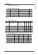
Document History Information
Version Date Descriptions
Ver. 1.0.0 Mar2011 Released with W5200 Launching
Ver. 1.1.0
13MAR2011
1.Changed “IMR address (0x16 to 0x36)” (P.14, P.18)
2.Changed “IMR2 address (0x36 to 0x16)” (P.14, P.22)
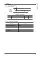
Ver. 1.2.0 22APR2011 1. Corrected description of “RSV at 1.3 Miscellaneous Signals” (P.10)
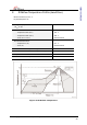
2. Corrected the values of “typical at 7.3 power dissipation” (P.77)
3. Added values of “maximum at 7.3 power dissipation ”(P.77)
4. Removed “PIN31 at 1.3 Miscellaneous Signals” ( P.10)
Ver. 1.2.1 2AUG2011 Corrected the description of “READ processing at 6.3 Processing of
using general SPI Master device ”(P.73)
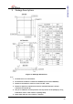
Ver. 1.2.2 25NOV2011 Corrected “Block Diagram” (P.4)
Ver. 1.2.3 3FEB2012 Added “Figure2 of XTAL_VDD at 1.4 Power Supply Signals” (P.11)
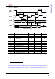
Ver. 1.2.4 16FEB2012 Corrected “Pin names and sequence diagrams of READ processing and
WRITE processing at 6.3 Processing of using general SPI Master
device” (P.73, 75)
Ver. 1.2.5 12APR2012 1. Corrected some miss phrase and words.
2. Corrected “Figure18 of SPI frame format at 6.1 SPI mode”(P.72)
Ver. 1.2.6 4JUN2012
1. Corrected value of “memory map at 2 Memory Map” (P.13)
2. Corrected code of “write processing at 6.3 Process of using general
SPI Master device” (P.75)
corrected SpiSendData function location
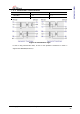
Ver. 1.2.7 27JULY2012 1.Updated “Pin names at 1 Pin Assignment” (P.8)
from PowerOut to 1V8O (PIN 14)
2.Changed “IMR address (0x36 to 0x16)” (P14, P.22-> P.18)
3.Changed “IMR2 address (0x16 to 0x36)” (P14, P.18->P.22)
4.Corrected table of “DIPR size format at 4.2 Socket Register” (P.33)
5.Corrected the table and figure of “RX, TX memory size format at 4.2
Socket Register
” (P.35,41)