
Data Sheet

© Copyright 2013 WIZnet Co.,Ltd. All rights reserved.
77
iEthernet
W5200
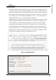
WRITE Processing
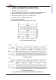
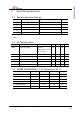
The WRITE Processing Sequence Diagram is shown in Figure 21.The WRITE processing is
entered by driving CSn low, followed by the Address, the OP code, the Data Length, and
the Data byte on MOSI.
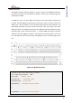
In W5200 SPI mode, the Byte WRITE processing and the Burst WRITE processing are
provided. The Byte WRITE processing takes 4 instructions which is consist of the 16-bit
Address, the 1-bit OP code(0x1), the 15-bit Data length and 8-bit Data. Otherwise, The
Burst WRITE processing only takes the Data instruction after the setting of the Burst
WRITE processing. To distinguish between the Byte WRITE and the Burst WRITE processing,
the Data length is used. If the Data length is ‘1,’ the Byte WRITE processing is operated.
Otherwise, the Burst WRITE Processing is operated when the Data length is more than
two. The MOSI pin should be selected by driving MOSI low after the falling edge of the
CSn.
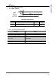
Figure 22 Write Sequence
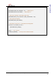
/* Pseudo Code for Write data of 8bit per packet */
#define data_write_command 0x80
uint16 addr; // Address : 16bits
int16 data_len; // Data length :15bits
uint8 data_buf[]; // Array for data
SpiSendData(); //Send data from MCU to W5200
{
ISR_DISABLE();// Interrupt Service Routine disable