
Data Sheet


© Copyright 2013 WIZnet Co.,Ltd. All rights reserved.
7
iEthernet
W5200
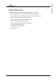
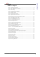
Table of Figure
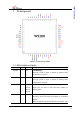
Figure 1 Pin Description W5200 .................................................................. 8
Figure 2 XTAL_VDD Reference Schematic .................................................... 11
Figure 3 Power Design ........................................................................... 12
Figure 4 Crystal Reference Schematic ........................................................ 13
Figure 5 INTLEVEL Timing ....................................................................... 21
Figure 6 Socket Status Transition .............................................................. 33
Figure 7 Physical Address Calculation ......................................................... 39
Figure 8 Allocation Internal TX/RX memory of Socket n ................................... 45
Figure 9 TCP SERVER and TCP CLIENT ......................................................... 46
Figure 10 TCP SERVER Operation Flow ........................................................ 47
Figure 11 TCP CLIENT Operation Flow ........................................................ 54
Figure 12 UDP Operation Flow .................................................................. 55
Figure 13 The Received UDP data Format .................................................... 57
Figure 14 IPRAW Operation Flow ............................................................... 65
Figure 15 The receive IPRAW data Format ................................................... 66
Figure 16 MACRAW Operation Flow ............................................................ 67
Figure 17 The received MACRAW data Format ............................................. 68
Figure 18 SPI Interface ........................................................................... 73
Figure 19 W5200 SPI Frame Format ........................................................... 74
Figure 20 Address and OP/DATA Length Sequence Diagram ............................... 74
Figure 21 READ Sequence ....................................................................... 75
Figure 22 Write Sequence ....................................................................... 77
Figure 23 Reset Timing ........................................................................... 80
Figure 24 SPI Timing .............................................................................. 81
Figure 25 Transformer Type ..................................................................... 82
Figure 26 IR Reflow Temperature .............................................................. 83
Figure 27 Package Dimensions .................................................................. 84