
Data Sheet
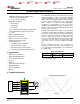

DRV8825
SLVSA73F –APRIL 2010–REVISED JULY 2014
www.ti.com
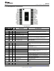
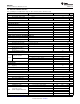
Pin Functions (continued)
PIN
EXTERNAL COMPONENTS
I/O
(1)
DESCRIPTION
OR CONNECTIONS
NAME NO.
nHOME 27 OD Home position Logic low when at home state of step table
OUTPUT
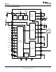
AOUT1 5 O Bridge A output 1
Connect to bipolar stepper motor winding A.
Positive current is AOUT1 → AOUT2
AOUT2 7 O Bridge A output 2
BOUT1 10 O Bridge B output 1
Connect to bipolar stepper motor winding B.
Positive current is BOUT1 → BOUT2
BOUT2 8 O Bridge B output 2
ISENA 6 I/O Bridge A ground / Isense Connect to current sense resistor for bridge A.
ISENB 9 I/O Bridge B ground / Isense Connect to current sense resistor for bridge B.
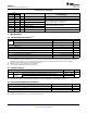
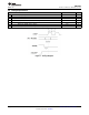
7 Specifications
7.1 Absolute Maximum Ratings
(1)(2)
MIN MAX UNIT
Power supply voltage –0.3 47 V
V
(VMx)
Power supply ramp rate 1 V/µs
Digital pin voltage –0.5 7 V
V
(xVREF)
Input voltage –0.3 4 V
ISENSEx pin voltage
(3)
–0.8 0.8 V
Peak motor drive output current, t < 1 μs Internally limited A
Continuous motor drive output current
(4)
0 2.5 A
Continuous total power dissipation See Thermal Information
T
J
Operating junction temperature range –40 150 °C
(1) Stresses beyond those listed under Absolute Maximum Ratings may cause permanent damage to the device. These are stress ratings
only, and functional operation of the device at these or any other conditions beyond those indicated under Recommended Operating
Conditions is not implied. Exposure to absolute-maximum-rated conditions for extended periods may affect device reliability.
(2) All voltage values are with respect to network ground terminal.
(3) Transients of ± 1 V for less than 25 ns are acceptable
(4) Power dissipation and thermal limits must be observed.
7.2 Handling Ratings
MIN MAX UNIT
T
stg
Storage temperature range –60 150 °C
Human body model (HBM), per ANSI/ESDA/JEDEC JS-001, all pins
(1)
–2000 2000
Electrostatic
V
(ESD)
V
discharge
Charged device model (CDM), per JEDEC specification JESD22-C101, all pins
(2)
–500 500
(1) JEDEC document JEP155 states that 500-V HBM allows safe manufacturing with a standard ESD control process.
(2) JEDEC document JEP157 states that 250-V CDM allows safe manufacturing with a standard ESD control process.
7.3 Recommended Operating Conditions
MIN NOM MAX UNIT
V
(VMx)
Motor power supply voltage range
(1)
8.2 45 V
V
(VREF)
VREF input voltage
(2)
1 3.5 V
I
V3P3
V3P3OUT load current 0 1 mA
(1) All V
M
pins must be connected to the same supply voltage.
(2) Operational at VREF between 0 to 1 V, but accuracy is degraded.
4 Submit Documentation Feedback Copyright © 2010–2014, Texas Instruments Incorporated
Product Folder Links: DRV8825