
Data Sheet


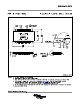

0.1 µF
0.01 µF
CP1
GND
CP2
VCP
VMA
AOUT1
ISENA
AOUT2
BOUT2
ISENB
BOUT1
VMB
AVREF
nHOME
MODE2
MODE1
MODE0
NC
STEP
nENBL
DIR
DECAY
nFAULT
nSLEEP
BVREF
GND
nRESET
V3P3OUT
0.47 µF
0.1 µF
0.1 µF
+
R
ISENA
R
ISENB
1 M
DRV8825
SLVSA73F –APRIL 2010–REVISED JULY 2014
www.ti.com
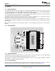
11 Layout
11.1 Layout Guidelines
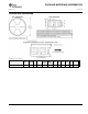
The VMA and VMB pins should be bypassed to GND using low-ESR ceramic bypass capacitors with a
recommended value of 0.1-μF rated for VMx. This capacitor should be placed as close to the VMA and VMB pins
as possible with a thick trace or ground plane connection to the device GND pin.
The VMA and VMB pins must be bypassed to ground using an appropriate bulk capacitor. This component may
be an electrolytic and should be located close to the DRV8825.
A low-ESR ceramic capacitor must be placed in between the CPL and CPH pins. TI recommends a value of
0.01-μF rated for VMx. Place this component as close to the pins as possible.
A low-ESR ceramic capacitor must be placed in between the VMA and VCP pins. TI recommends a value of 0.1-
μF rated for 16 V. Place this component as close to the pins as possible. Also, place a 1-MΩ resistor between
VCP and VMA.
Bypass V3P3 to ground with a ceramic capacitor rated 6.3 V. Place this bypass capacitor as close to the pin as
possible
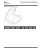
11.2 Layout Example
11.3 Thermal Protection
The DRV8825 has thermal shutdown (TSD) as described above. If the die temperature exceeds approximately
150°C, the device will be disabled until the temperature drops to a safe level.
Any tendency of the device to enter TSD is an indication of either excessive power dissipation, insufficient
heatsinking, or too high an ambient temperature.
11.3.1 Power Dissipation
Power dissipation in the DRV8825 is dominated by the power dissipated in the output FET resistance, or R
DS(ON)
.
Average power dissipation when running a stepper motor can be roughly estimated by Equation 5.
22 Submit Documentation Feedback Copyright © 2010–2014, Texas Instruments Incorporated
Product Folder Links: DRV8825