
Data Sheet


Datasheet
5A 350KHz 25V Buck DC to DC Converter
2
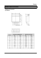
Pin Configurations
Figure2. Pin Configuration of GS2678 (Top View)
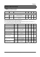
Table 1 Pin Description
Pin Number Pin Name Description
1 GND
Ground Pin. Care must be taken in layout. This pin should be
placed outside of the Schottky Diode to output capacitor
ground path to prevent switching current spikes from inducing
voltage noise into GS2678.
2 FB
Feedback Pin (FB). Through an external resistor divider
network, FB senses the output voltage and regulates it. The
feedback threshold voltage is 0.8V.
3 SW
Power Switch Output Pin (SW). SW is the switch node that
supplies power to the output.
4 EN
Enable Pin. Drive EN pin high to turn on the device, drive it
low to turn it off. Floating is default high.
5 VIN
Supply Voltage Input Pin. GS2678 operates from a 3.6V to
25V DC voltage. Bypass Vin to GND with a suitably large
capacitor to eliminate noise on the input.
SHENZHEN GSM ELECTAONIC CO.,LTD http://www.086ic.cn tel:0755-81275006 mob:13424297678