
Data Sheet

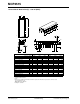
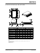
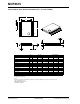

Table Of Contents
- 1.0 Device Overview
- 2.0 Can Message Frames
- 3.0 Message Transmission
- 4.0 Message Reception
- 5.0 Bit Timing
- 6.0 Error Detection
- 7.0 Interrupts
- 8.0 Oscillator
- 9.0 RESET
- 10.0 Modes of Operation
- 11.0 Register Map
- 12.0 SPI™ Interface
- 12.1 Overview
- 12.2 Reset Instruction
- 12.3 Read Instruction
- 12.4 Read RX Buffer Instruction
- 12.5 Write Instruction
- 12.6 Load TX Buffer Instruction
- 12.7 Request-To-Send (RTS) Instruction
- 12.8 Read Status Instruction
- 12.9 RX Status Instruction
- 12.10 Bit Modify Instruction
- Figure 12-1: Bit Modify
- Table 12-1: SPI™ Instruction Set
- Figure 12-2: Read instruction
- Figure 12-3: Read RX Buffer Instruction
- Figure 12-4: Byte Write instruction
- Figure 12-5: Load TX Buffer
- Figure 12-6: Request-to-send (RTS) instruction
- Figure 12-7: BIT Modify instruction
- Figure 12-8: Read Status instruction
- Figure 12-9: RX StatUs Instruction
- Figure 12-10: SPI™ Input Timing
- Figure 12-11: SPI™ Output TIming
- 13.0 Electrical Characteristics
- 14.0 PackAging Information

© 2005 Microchip Technology Inc. Preliminary DS21801D-page 79
MCP2515
APPENDIX A: REVISION HISTORY
Revision D (April 2005)
The following is the list of modifications:
1. Section 8.0. Added Table 8-1 and Table 8-2.
Added note box following tables.
2. Section 11.0, Table 11-1. Changed address bits
in column heading.
3. Modified Section 14.0 Packaging Information to
reflect pb free device markings.
4. Appendix A Revision History: Rearranged order
of importance.
Revision C (November 2004)
The following is the list of modifications:
1. New section 9.0 added.
2. Section 12, Heading 12.1: added notebox.
Heading 12.6: Changed verbiage within
paragraph.
3. Added Appendix A: Revision History.
Revision B (September 2003)
The following is the list of modifications:
1. Front page bullet: Standby current (typical)
(Sleep Mode) changed from 10 µA to 1 µA
2. Section 8.2 CLKOUT Pin: Added notebox for
maximum frequency on CLKOUT.
3. Section 12.0, Table 12-1:
- Changed supply voltage minimum to 2.7V.
- Internal Capacitance: Changed V
DD
condition to 0V.
- Standby Current (Sleep mode): Split
specification into -40°C to +85°C and
-40°C to +125°C.
Revision A (May 2003)
• Original Relase of this Document.