
Data Sheet
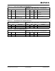
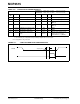
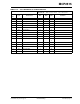

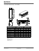
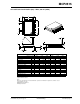
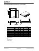

Table Of Contents
- 1.0 Device Overview
- 2.0 Can Message Frames
- 3.0 Message Transmission
- 4.0 Message Reception
- 5.0 Bit Timing
- 6.0 Error Detection
- 7.0 Interrupts
- 8.0 Oscillator
- 9.0 RESET
- 10.0 Modes of Operation
- 11.0 Register Map
- 12.0 SPI™ Interface
- 12.1 Overview
- 12.2 Reset Instruction
- 12.3 Read Instruction
- 12.4 Read RX Buffer Instruction
- 12.5 Write Instruction
- 12.6 Load TX Buffer Instruction
- 12.7 Request-To-Send (RTS) Instruction
- 12.8 Read Status Instruction
- 12.9 RX Status Instruction
- 12.10 Bit Modify Instruction
- Figure 12-1: Bit Modify
- Table 12-1: SPI™ Instruction Set
- Figure 12-2: Read instruction
- Figure 12-3: Read RX Buffer Instruction
- Figure 12-4: Byte Write instruction
- Figure 12-5: Load TX Buffer
- Figure 12-6: Request-to-send (RTS) instruction
- Figure 12-7: BIT Modify instruction
- Figure 12-8: Read Status instruction
- Figure 12-9: RX StatUs Instruction
- Figure 12-10: SPI™ Input Timing
- Figure 12-11: SPI™ Output TIming
- 13.0 Electrical Characteristics
- 14.0 PackAging Information
MCP2515
DS21801D-page 78 Preliminary © 2005 Microchip Technology Inc.
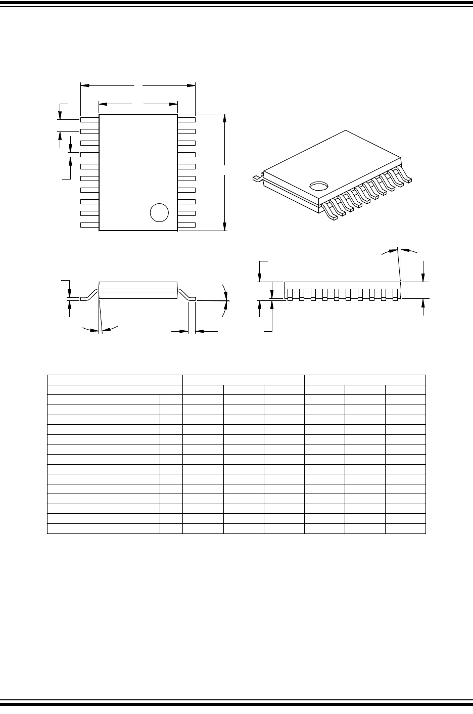
20-Lead Plastic Thin Shrink Small Outline (ST) – 4.4 mm (TSSOP)
Foot Angle
φ
048048
10501050
β
Mold Draft Angle Bottom
10501050
α
Mold Draft Angle Top
0.300.250.19.012.010.007BLead Width
0.200.150.09.008.006.004
c
Lead Thickness
0.700.600.50.028.024.020LFoot Length
6.606.506.40.260.256.252DMolded Package Length
4.504.404.30.177.173.169E1Molded Package Width
6.506.386.25.256.251.246EOverall Width
0.150.100.05.006.004.002A1Standoff §
0.950.900.85.037.035.033A2Molded Package Thickness
1.10.043AOverall Height
0.65.026
p
Pitch
2020
n
Number of Pins
MAXNOMMINMAXNOMMIN
Dimension Limits
MILLIMETERS*INCHESUnits
1
2
D
p
n
B
E1
E
L
β
c
φ
α
A2
A1
A
* Controlling Parameter
Notes:
Dimensions D and E1 do not include mold flash or protrusions. Mold flash or protrusions shall not exceed
.005” (0.127mm) per side.
JEDEC Equivalent: MO-153
Drawing No. C04-088
§ Significant Characteristic