
Data Sheet

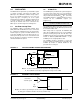
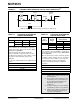


Table Of Contents
- 1.0 Device Overview
- 2.0 Can Message Frames
- 3.0 Message Transmission
- 4.0 Message Reception
- 5.0 Bit Timing
- 6.0 Error Detection
- 7.0 Interrupts
- 8.0 Oscillator
- 9.0 RESET
- 10.0 Modes of Operation
- 11.0 Register Map
- 12.0 SPI™ Interface
- 12.1 Overview
- 12.2 Reset Instruction
- 12.3 Read Instruction
- 12.4 Read RX Buffer Instruction
- 12.5 Write Instruction
- 12.6 Load TX Buffer Instruction
- 12.7 Request-To-Send (RTS) Instruction
- 12.8 Read Status Instruction
- 12.9 RX Status Instruction
- 12.10 Bit Modify Instruction
- Figure 12-1: Bit Modify
- Table 12-1: SPI™ Instruction Set
- Figure 12-2: Read instruction
- Figure 12-3: Read RX Buffer Instruction
- Figure 12-4: Byte Write instruction
- Figure 12-5: Load TX Buffer
- Figure 12-6: Request-to-send (RTS) instruction
- Figure 12-7: BIT Modify instruction
- Figure 12-8: Read Status instruction
- Figure 12-9: RX StatUs Instruction
- Figure 12-10: SPI™ Input Timing
- Figure 12-11: SPI™ Output TIming
- 13.0 Electrical Characteristics
- 14.0 PackAging Information
© 2005 Microchip Technology Inc. Preliminary DS21801D-page 53
MCP2515
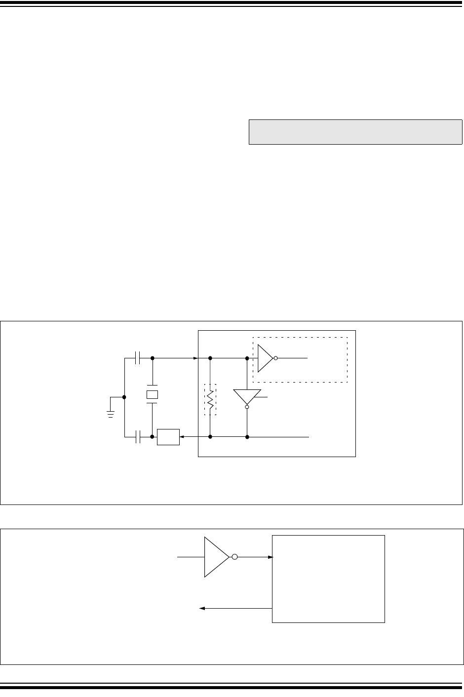
8.0 OSCILLATOR
The MCP2515 is designed to be operated with a crystal
or ceramic resonator connected to the OSC1 and
OSC2 pins. The MCP2515 oscillator design requires
the use of a parallel cut crystal. Use of a series cut
crystal may give a frequency out of the crystal
manufacturers specifications. A typical oscillator circuit
is shown in Figure 8-1. The MCP2515 may also be
driven by an external clock source connected to the
OSC1 pin, as shown in Figure 8-2 and Figure 8-3.
8.1 Oscillator Startup Timer
The MCP2515 utilizes an Oscillator Startup Timer
(OST) that holds the MCP2515 in reset to ensure that
the oscillator has stabilized before the internal state
machine begins to operate. The OST maintains reset
for the first 128 OSC1 clock cycles after power-up or a
wake-up from Sleep mode occurs. It should be noted
that no SPI protocol operations should be attempted
until after the OST has expired.
8.2 CLKOUT Pin
The CLKOUT pin is provided to the system designer for
use as the main system clock or as a clock input for
other devices in the system. The CLKOUT has an inter-
nal prescaler which can divide F
OSC
by 1, 2, 4 and 8.
The CLKOUT function is enabled and the prescaler is
selected via the CANCNTRL register (see
Register 10-1).
The CLKOUT pin will be active upon system reset and
default to the slowest speed (divide by 8) so that it can
be used as the MCU clock.
When Sleep mode is requested, the MCP2515 will
drive sixteen additional clock cycles on the CLKOUT
pin before entering Sleep mode. The idle state of the
CLKOUT pin in Sleep mode is low. When the CLKOUT
function is disabled (CANCNTRL.CLKEN = ‘0’) the
CLKOUT pin is in a high-impedance state.
The CLKOUT function is designed to ensure that
t
hCLKOUT
and t
lCLKOUT
timings are preserved when the
CLKOUT pin function is enabled, disabled or the
prescaler value is changed.
FIGURE 8-1: CRYSTAL/CERAMIC RESONATOR OPERATION
FIGURE 8-2: EXTERNAL CLOCK SOURCE
Note: The maximum frequency on CLKOUT is
specified as 25 MHz (See Table 13-5)
C
1
C
2
XTAL
OSC2
RS
(1)
OSC1
RF
(2)
SLEEP
To internal logic
Note 1: A series resistor (RS) may be required for AT strip cut crystals.
2: The feedback resistor (R
F), is typically in the range of 2 to 10 MΩ.
Clock from
external system
OSC1
OSC2
Open
(1)
Note 1: A resistor to ground may be used to reduce system noise. This may increase system current.
2: Duty cycle restrictions must be observed (see Table 12-2).