
Data Sheet
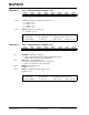
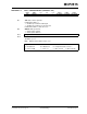

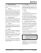
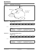

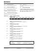
Table Of Contents
- 1.0 Device Overview
- 2.0 Can Message Frames
- 3.0 Message Transmission
- 4.0 Message Reception
- 5.0 Bit Timing
- 6.0 Error Detection
- 7.0 Interrupts
- 8.0 Oscillator
- 9.0 RESET
- 10.0 Modes of Operation
- 11.0 Register Map
- 12.0 SPI™ Interface
- 12.1 Overview
- 12.2 Reset Instruction
- 12.3 Read Instruction
- 12.4 Read RX Buffer Instruction
- 12.5 Write Instruction
- 12.6 Load TX Buffer Instruction
- 12.7 Request-To-Send (RTS) Instruction
- 12.8 Read Status Instruction
- 12.9 RX Status Instruction
- 12.10 Bit Modify Instruction
- Figure 12-1: Bit Modify
- Table 12-1: SPI™ Instruction Set
- Figure 12-2: Read instruction
- Figure 12-3: Read RX Buffer Instruction
- Figure 12-4: Byte Write instruction
- Figure 12-5: Load TX Buffer
- Figure 12-6: Request-to-send (RTS) instruction
- Figure 12-7: BIT Modify instruction
- Figure 12-8: Read Status instruction
- Figure 12-9: RX StatUs Instruction
- Figure 12-10: SPI™ Input Timing
- Figure 12-11: SPI™ Output TIming
- 13.0 Electrical Characteristics
- 14.0 PackAging Information
MCP2515
DS21801D-page 46 Preliminary © 2005 Microchip Technology Inc.
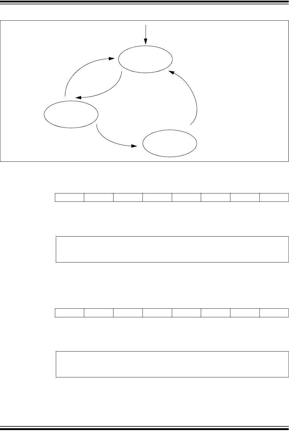
FIGURE 6-1: ERROR MODES STATE DIAGRAM
REGISTER 6-1: TEC – TRANSMIT ERROR COUNTER
(ADDRESS: 1Ch)
REGISTER 6-2: REC – RECEIVER ERROR COUNTER
(ADDRESS: 1Dh)
R-0 R-0 R-0 R-0 R-0 R-0 R-0 R-0
TEC7 TEC6 TEC5 TEC4 TEC3 TEC2 TEC1 TEC0
bit 7 bit 0
bit 7-0 TEC: Transmit Error Count bits <7:0>
Legend:
R = Readable bit W = Writable bit U = Unimplemented bit, read as ‘0’
-n = Value at POR ‘1’ = Bit is set ‘0’ = Bit is cleared x = Bit is unknown
R-0 R-0 R-0 R-0 R-0 R-0 R-0 R-0
REC7 REC6 REC5 REC4 REC3 REC2 REC1 REC0
bit 7 bit 0
bit 7-0 REC: Receive Error Count bits <7:0>
Legend:
R = Readable bit W = Writable bit U = Unimplemented bit, read as ‘0’
-n = Value at POR ‘1’ = Bit is set ‘0’ = Bit is cleared x = Bit is unknown
Bus-Off
Error-Active
Error-Passive
REC < 127 or
TEC < 127
REC > 127 or
TEC > 127
TEC > 255
RESET
128 occurrences of
11 consecutive
“recessive” bits