
Data Sheet
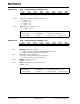


Table Of Contents
- 1.0 Device Overview
- 2.0 Can Message Frames
- 3.0 Message Transmission
- 4.0 Message Reception
- 5.0 Bit Timing
- 6.0 Error Detection
- 7.0 Interrupts
- 8.0 Oscillator
- 9.0 RESET
- 10.0 Modes of Operation
- 11.0 Register Map
- 12.0 SPI™ Interface
- 12.1 Overview
- 12.2 Reset Instruction
- 12.3 Read Instruction
- 12.4 Read RX Buffer Instruction
- 12.5 Write Instruction
- 12.6 Load TX Buffer Instruction
- 12.7 Request-To-Send (RTS) Instruction
- 12.8 Read Status Instruction
- 12.9 RX Status Instruction
- 12.10 Bit Modify Instruction
- Figure 12-1: Bit Modify
- Table 12-1: SPI™ Instruction Set
- Figure 12-2: Read instruction
- Figure 12-3: Read RX Buffer Instruction
- Figure 12-4: Byte Write instruction
- Figure 12-5: Load TX Buffer
- Figure 12-6: Request-to-send (RTS) instruction
- Figure 12-7: BIT Modify instruction
- Figure 12-8: Read Status instruction
- Figure 12-9: RX StatUs Instruction
- Figure 12-10: SPI™ Input Timing
- Figure 12-11: SPI™ Output TIming
- 13.0 Electrical Characteristics
- 14.0 PackAging Information
© 2005 Microchip Technology Inc. Preliminary DS21801D-page 43
MCP2515
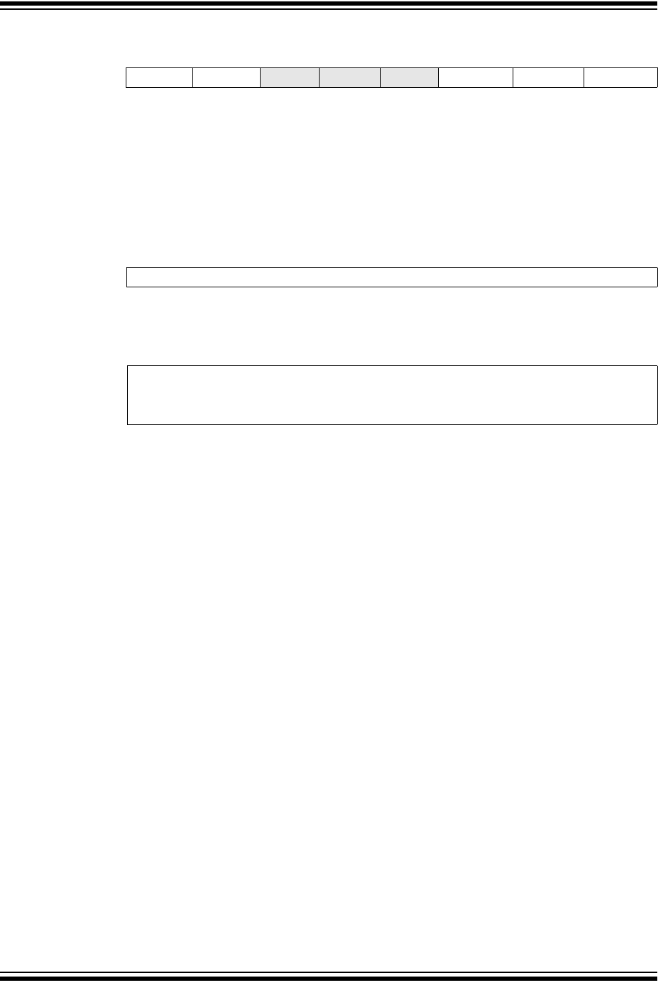
REGISTER 5-3: CNF3 - CONFIGURATION 1 (ADDRESS: 28h)
R/W-0 R/W-0 U-0 U-0 U-0 R/W-0 R/W-0 R/W-0
SOF WAKFIL — — — PHSEG22 PHSEG21 PHSEG20
bit 7 bit 0
bit 7 SOF: Start-of-Frame signal bit
If CANCTRL.CLKEN = 1:
1 = CLKOUT pin enabled for SOF signal
0 = CLKOUT pin enabled for clockout function
If CANCTRL.CLKEN = 0, Bit is don’t care.
bit 6 WAKFIL: Wake-up Filter bit
1 = Wake-up filter enabled
0 = Wake-up filter disabled
bit 5-3 Unimplemented: Reads as ‘0’
bit 2-0 PHSEG2: PS2 Length bits<2:0>
(PHSEG2 + 1) x T
Q
Note: Minimum valid setting for PS2 is 2 TQ
Legend:
R = Readable bit W = Writable bit U = Unimplemented bit, read as ‘0’
-n = Value at POR ‘1’ = Bit is set ‘0’ = Bit is cleared x = Bit is unknown