
Data Sheet
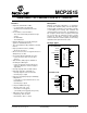
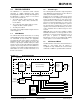
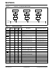
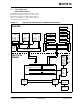
Table Of Contents
- 1.0 Device Overview
- 2.0 Can Message Frames
- 3.0 Message Transmission
- 4.0 Message Reception
- 5.0 Bit Timing
- 6.0 Error Detection
- 7.0 Interrupts
- 8.0 Oscillator
- 9.0 RESET
- 10.0 Modes of Operation
- 11.0 Register Map
- 12.0 SPI™ Interface
- 12.1 Overview
- 12.2 Reset Instruction
- 12.3 Read Instruction
- 12.4 Read RX Buffer Instruction
- 12.5 Write Instruction
- 12.6 Load TX Buffer Instruction
- 12.7 Request-To-Send (RTS) Instruction
- 12.8 Read Status Instruction
- 12.9 RX Status Instruction
- 12.10 Bit Modify Instruction
- Figure 12-1: Bit Modify
- Table 12-1: SPI™ Instruction Set
- Figure 12-2: Read instruction
- Figure 12-3: Read RX Buffer Instruction
- Figure 12-4: Byte Write instruction
- Figure 12-5: Load TX Buffer
- Figure 12-6: Request-to-send (RTS) instruction
- Figure 12-7: BIT Modify instruction
- Figure 12-8: Read Status instruction
- Figure 12-9: RX StatUs Instruction
- Figure 12-10: SPI™ Input Timing
- Figure 12-11: SPI™ Output TIming
- 13.0 Electrical Characteristics
- 14.0 PackAging Information
MCP2515
DS21801D-page 4 Preliminary © 2005 Microchip Technology Inc.
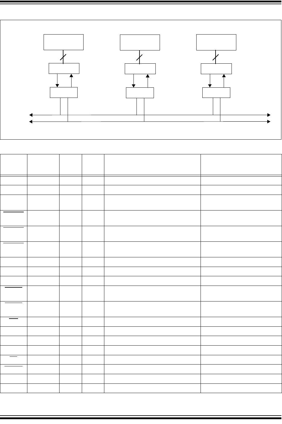
FIGURE 1-2: EXAMPLE SYSTEM IMPLEMENTATION
TABLE 1-1: PINOUT DESCRIPTION
Name
PDIP/SOIC
Pin #
TSSOP
Pin #
I/O/P
Type
Description Alternate Pin Function
TXCAN 1 1 O Transmit output pin to CAN bus —
RXCAN 2 2 I Receive input pin from CAN bus —
CLKOUT 3 3 O Clock output pin with programmable
prescaler
Start-of-Frame signal
TX0RTS
4 4 I Transmit buffer TXB0 request-to-send.
100 kΩ internal pull-up to V
DD
General purpose digital input.
100 kΩ internal pull-up to V
DD
TX1RTS 5 5 I Transmit buffer TXB1 request-to-send.
100 kΩ internal pull-up to V
DD
General purpose digital input.
100 kΩ internal pull-up to V
DD
TX2RTS 6 7 I Transmit buffer TXB2 request-to-send.
100 kΩ internal pull-up to V
DD
General purpose digital input.
100 kΩ internal pull-up to V
DD
OSC2 7 8 O Oscillator output —
OSC1 8 9 I Oscillator input External clock input
V
SS 9 10 P Ground reference for logic and I/O pins —
RX1BF
10 11 O Receive buffer RXB1 interrupt pin or
general purpose digital output
General purpose digital output
RX0BF
11 12 O Receive buffer RXB0 interrupt pin or
general purpose digital output
General purpose digital output
INT
12 13 O Interrupt output pin —
SCK 13 14 I Clock input pin for SPI™ interface —
SI 14 16 I Data input pin for SPI interface —
SO 15 17 O Data output pin for SPI interface —
CS 16 18 I Chip select input pin for SPI interface —
RESET 17 19 I Active low device reset input —
VDD 18 20 P Positive supply for logic and I/O pins —
NC — 6,15 — No internal connection
Note: Type Identification: I = Input; O = Output; P = Power
Node
Controller
MCP2515
XCVR
SPI™
TX
RX
CANH
CANL
Node
Controller
MCP2515
XCVR
SPI
TX
RX
Node
Controller
MCP2515
XCVR
SPI
TX
RX