
Data Sheet

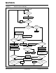
Table Of Contents
- 1.0 Device Overview
- 2.0 Can Message Frames
- 3.0 Message Transmission
- 4.0 Message Reception
- 5.0 Bit Timing
- 6.0 Error Detection
- 7.0 Interrupts
- 8.0 Oscillator
- 9.0 RESET
- 10.0 Modes of Operation
- 11.0 Register Map
- 12.0 SPI™ Interface
- 12.1 Overview
- 12.2 Reset Instruction
- 12.3 Read Instruction
- 12.4 Read RX Buffer Instruction
- 12.5 Write Instruction
- 12.6 Load TX Buffer Instruction
- 12.7 Request-To-Send (RTS) Instruction
- 12.8 Read Status Instruction
- 12.9 RX Status Instruction
- 12.10 Bit Modify Instruction
- Figure 12-1: Bit Modify
- Table 12-1: SPI™ Instruction Set
- Figure 12-2: Read instruction
- Figure 12-3: Read RX Buffer Instruction
- Figure 12-4: Byte Write instruction
- Figure 12-5: Load TX Buffer
- Figure 12-6: Request-to-send (RTS) instruction
- Figure 12-7: BIT Modify instruction
- Figure 12-8: Read Status instruction
- Figure 12-9: RX StatUs Instruction
- Figure 12-10: SPI™ Input Timing
- Figure 12-11: SPI™ Output TIming
- 13.0 Electrical Characteristics
- 14.0 PackAging Information
© 2005 Microchip Technology Inc. Preliminary DS21801D-page 29
MCP2515
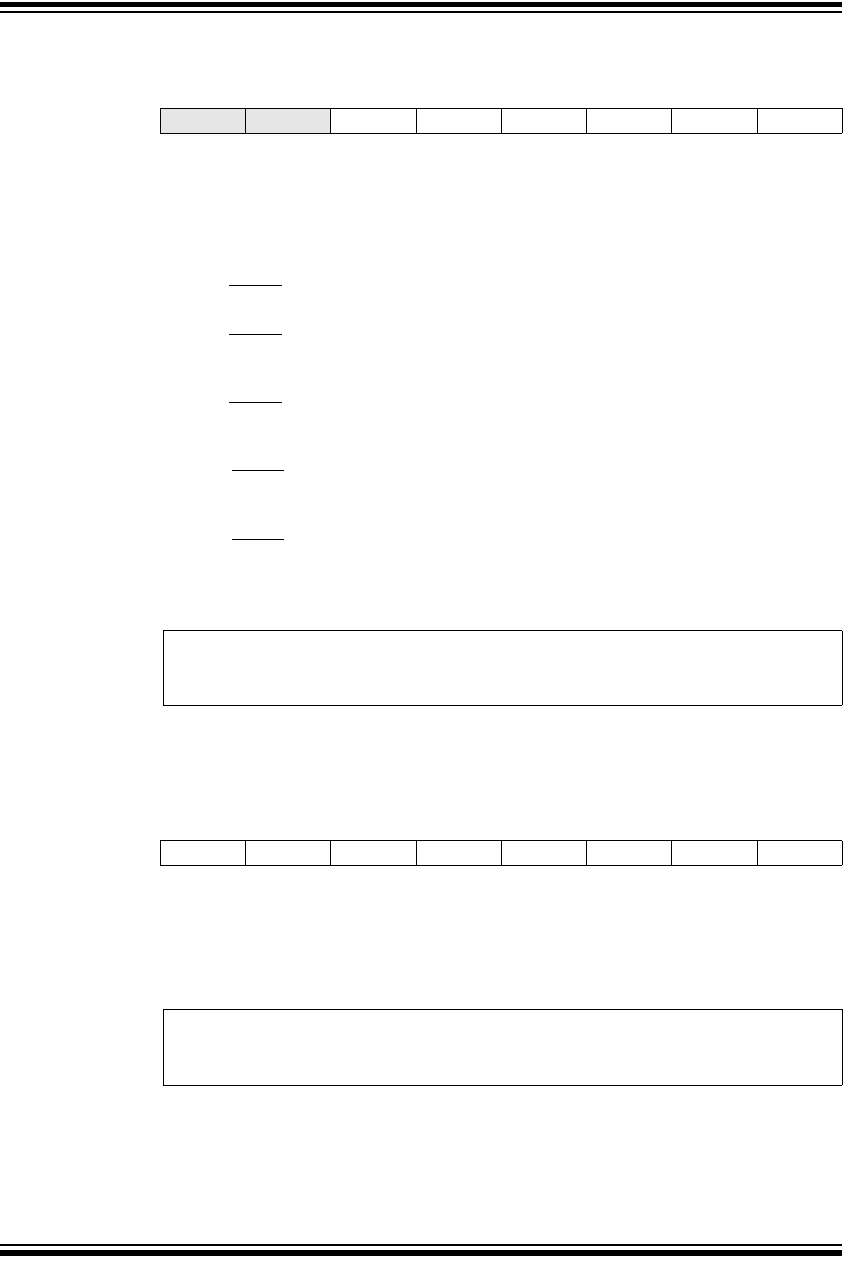
REGISTER 4-3: BFPCTRL – RXnBF PIN CONTROL AND STATUS
(ADDRESS: 0Ch)
REGISTER 4-4: RXBnSIDH – RECEIVE BUFFER n STANDARD IDENTIFIER HIGH
(ADDRESS: 61h, 71h)
U-0 U-0 R/W-0 R/W-0 R/W-0 R/W-0 R/W-0 R/W-0
— — B1BFS B0BFS B1BFE B0BFE B1BFM B0BFM
bit 7 bit 0
bit 7 Unimplemented: Read as ‘0’
bit 6 Unimplemented: Read as ‘0’
bit 5 B1BFS: RX1BF
Pin State bit (Digital Output mode only)
- Reads as ‘0’ when RX1BF is configured as interrupt pin
bit 4 B0BFS: RX0BF Pin State bit (Digital Output mode only)
- Reads as ‘0’ when RX0BF is configured as interrupt pin
bit 3 B1BFE: RX1BF Pin Function Enable bit
1 = Pin function enabled, operation mode determined by B1BFM bit
0 = Pin function disabled, pin goes to high-impedance state
bit 2 B0BFE: RX0BF
Pin Function Enable bit
1 = Pin function enabled, operation mode determined by B0BFM bit
0 = Pin function disabled, pin goes to high-impedance state
bit 1 B1BFM: RX1BF
Pin Operation Mode bit
1 = Pin is used as interrupt when valid message loaded into RXB1
0 = Digital Output mode
bit 0 B0BFM: RX0BF
Pin Operation Mode bit
1 = Pin is used as interrupt when valid message loaded into RXB0
0 = Digital Output mode
Legend:
R = Readable bit W = Writable bit U = Unimplemented bit, read as ‘0’
-n = Value at POR ‘1’ = Bit is set ‘0’ = Bit is cleared x = Bit is unknown
R-x R-x R-x R-x R-x R-x R-x R-x
SID10SID9SID8SID7SID6SID5SID4SID3
bit 7 bit 0
bit 7-0 SID: Standard Identifier bits <10:3>
These bits contain the eight most significant bits of the Standard Identifier for the received
message
Legend:
R = Readable bit W = Writable bit U = Unimplemented bit, read as ‘0’
-n = Value at POR ‘1’ = Bit is set ‘0’ = Bit is cleared x = Bit is unknown