
Data Sheet

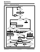
Table Of Contents
- 1.0 Device Overview
- 2.0 Can Message Frames
- 3.0 Message Transmission
- 4.0 Message Reception
- 5.0 Bit Timing
- 6.0 Error Detection
- 7.0 Interrupts
- 8.0 Oscillator
- 9.0 RESET
- 10.0 Modes of Operation
- 11.0 Register Map
- 12.0 SPI™ Interface
- 12.1 Overview
- 12.2 Reset Instruction
- 12.3 Read Instruction
- 12.4 Read RX Buffer Instruction
- 12.5 Write Instruction
- 12.6 Load TX Buffer Instruction
- 12.7 Request-To-Send (RTS) Instruction
- 12.8 Read Status Instruction
- 12.9 RX Status Instruction
- 12.10 Bit Modify Instruction
- Figure 12-1: Bit Modify
- Table 12-1: SPI™ Instruction Set
- Figure 12-2: Read instruction
- Figure 12-3: Read RX Buffer Instruction
- Figure 12-4: Byte Write instruction
- Figure 12-5: Load TX Buffer
- Figure 12-6: Request-to-send (RTS) instruction
- Figure 12-7: BIT Modify instruction
- Figure 12-8: Read Status instruction
- Figure 12-9: RX StatUs Instruction
- Figure 12-10: SPI™ Input Timing
- Figure 12-11: SPI™ Output TIming
- 13.0 Electrical Characteristics
- 14.0 PackAging Information
© 2005 Microchip Technology Inc. Preliminary DS21801D-page 25
MCP2515
4.4.3 CONFIGURED AS DIGITAL OUTPUT
When used as digital outputs, the BFPCTRL.BxBFM bit
must be cleared and BFPCTRL.BnBFE must be set for
the associated buffer. In this mode, the state of the pin
is controlled by the BFPCTRL.BnBFS bits. Writing a ‘1’
to the BnBFS bit will cause a high level to be driven on
the associated buffer full pin, while a ‘0’ will cause the
pin to drive low. When using the pins in this mode, the
state of the pin should be modified only by using the Bit
Modify SPI command to prevent glitches from
occurring on either of the buffer full pins.
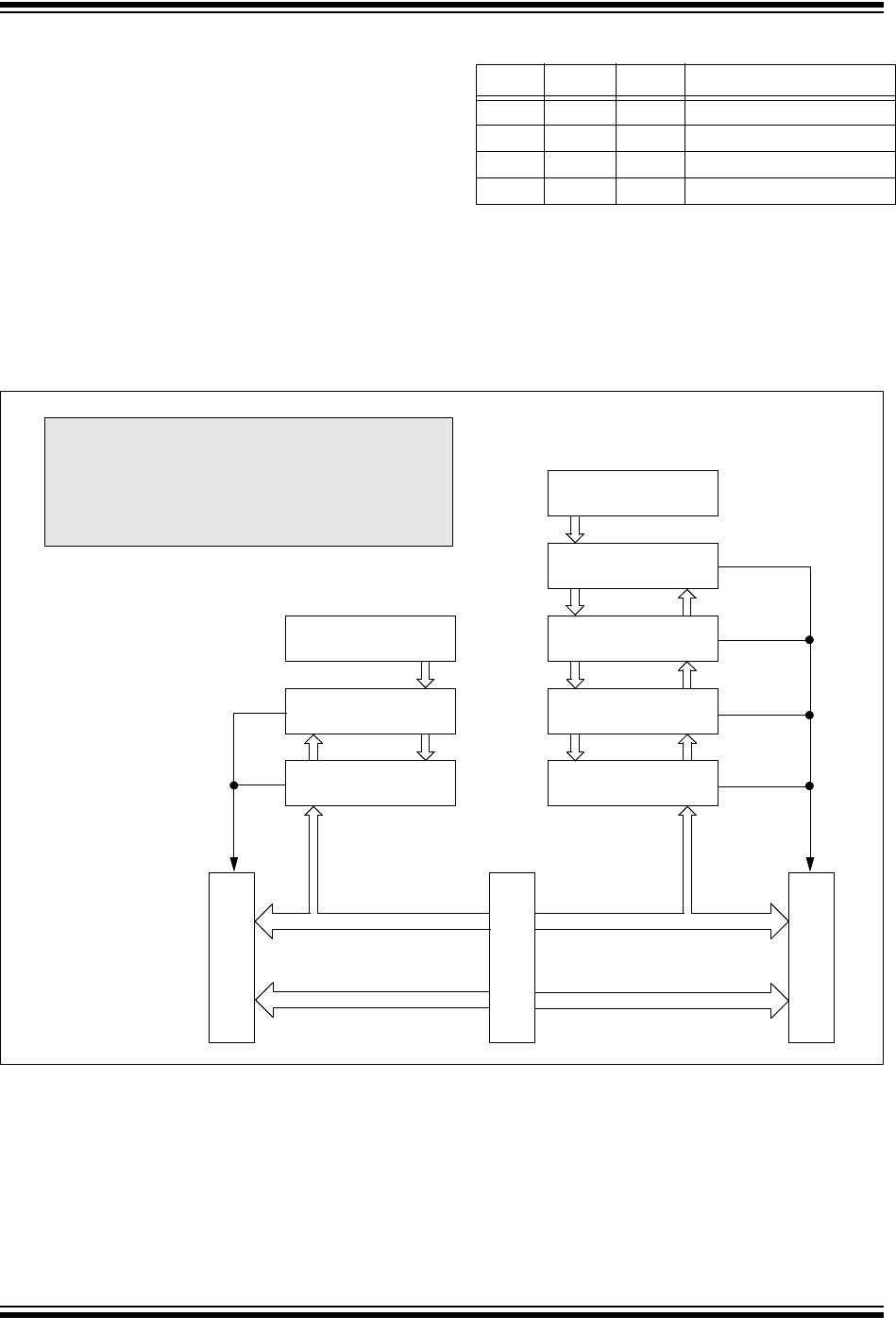
TABLE 4-1: CONFIGURING RXNBF PINS
FIGURE 4-2: RECEIVE BUFFER BLOCK DIAGRAM
BnBFE BnBFM BnBFS Pin Status
0XXDisabled, high-impedance
11XReceive buffer interrupt
100Digital output = 0
101Digital output = 1
Acceptance Mask
RXM1
Acceptance Filter
RXF2
Acceptance Filter
RXF3
Acceptance Filter
RXF4
Acceptance Filter
RXF5
Acceptance Mask
RXM0
Acceptance Filter
RXF0
Acceptance Filter
RXF1
Identifier
Data Field Data Field
Identifier
Note: Messages received in the MAB are intially
applied to the mask and filters of RXB0. In
addition, only one filter match occurs (e.g.,
if the message matches both RXF0 and
RXF2, the match will be for RXF0 and the
message will be moved into RXB0).
A
c
c
e
p
t
A
c
c
e
p
t
R
X
B
0
R
X
B
1
M
A
B