
Data Sheet

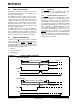
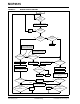
Table Of Contents
- 1.0 Device Overview
- 2.0 Can Message Frames
- 3.0 Message Transmission
- 4.0 Message Reception
- 5.0 Bit Timing
- 6.0 Error Detection
- 7.0 Interrupts
- 8.0 Oscillator
- 9.0 RESET
- 10.0 Modes of Operation
- 11.0 Register Map
- 12.0 SPI™ Interface
- 12.1 Overview
- 12.2 Reset Instruction
- 12.3 Read Instruction
- 12.4 Read RX Buffer Instruction
- 12.5 Write Instruction
- 12.6 Load TX Buffer Instruction
- 12.7 Request-To-Send (RTS) Instruction
- 12.8 Read Status Instruction
- 12.9 RX Status Instruction
- 12.10 Bit Modify Instruction
- Figure 12-1: Bit Modify
- Table 12-1: SPI™ Instruction Set
- Figure 12-2: Read instruction
- Figure 12-3: Read RX Buffer Instruction
- Figure 12-4: Byte Write instruction
- Figure 12-5: Load TX Buffer
- Figure 12-6: Request-to-send (RTS) instruction
- Figure 12-7: BIT Modify instruction
- Figure 12-8: Read Status instruction
- Figure 12-9: RX StatUs Instruction
- Figure 12-10: SPI™ Input Timing
- Figure 12-11: SPI™ Output TIming
- 13.0 Electrical Characteristics
- 14.0 PackAging Information
MCP2515
DS21801D-page 24 Preliminary © 2005 Microchip Technology Inc.
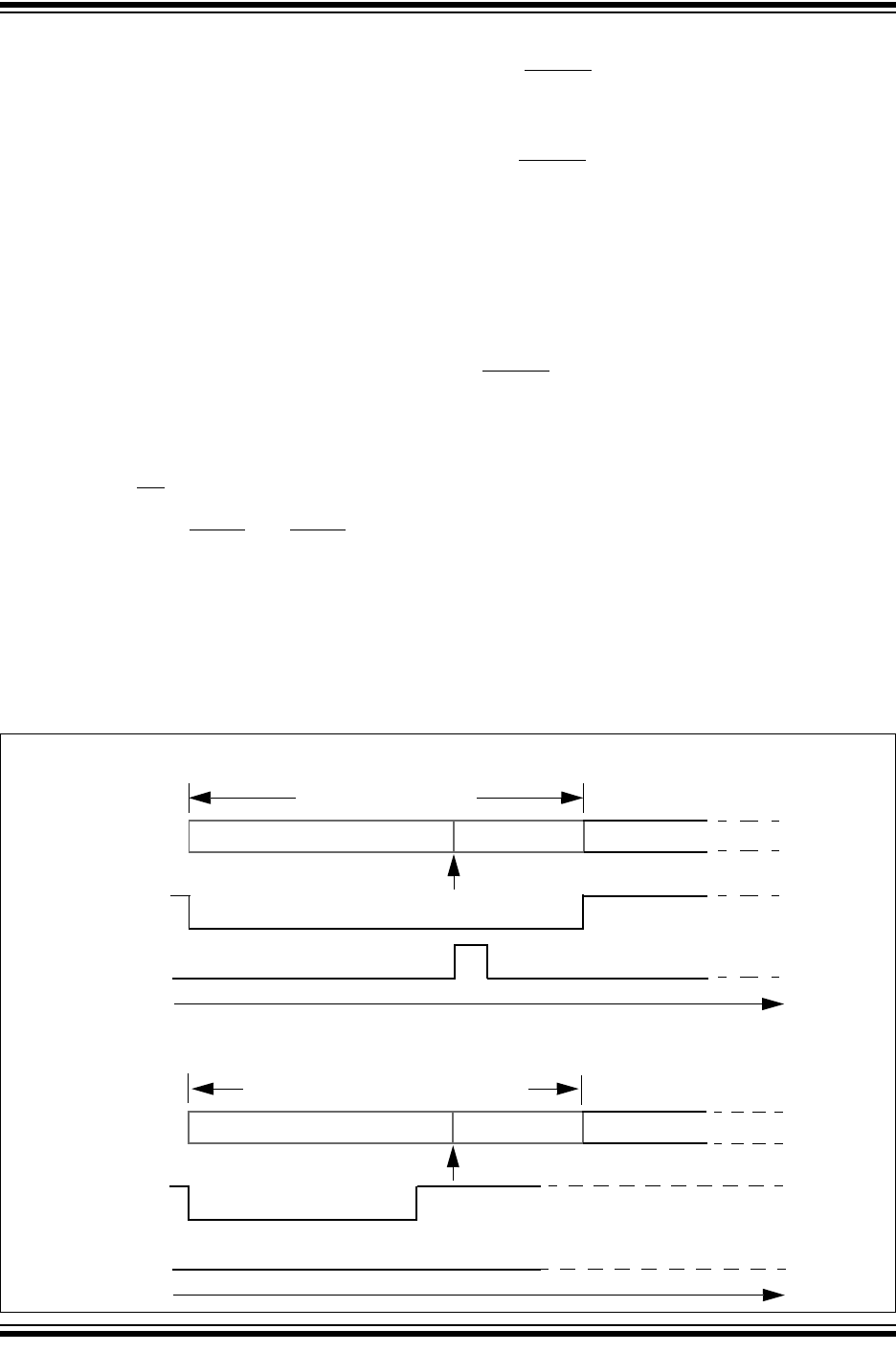
4.3 Start-of-Frame Signal
If enabled, the Start-Of-Frame signal is generated on
the SOF pin at the beginning of each CAN message
detected on the RXCAN pin.
The RXCAN pin monitors an idle bus for a recessive-
to-dominant edge. If the dominant condition remains
until the sample point, the MCP2515 interprets this as
a SOF and a SOF pulse is generated. If the dominant
condition does not remain until the sample point, the
MCP2515 interprets this as a glitch on the bus and no
SOF signal is generated. Figure 4-1 illustrates SOF
signalling and glitch-filtering.
As with One-shot mode, one use for SOF signaling is
for TTCAN-type systems. In addition, by monitoring
both the RXCAN pin and the SOF pin, a MCU can
detect early physical bus problems by detecting small
glitches before they affect the CAN communications.
4.4 RX0BF and RX1BF Pins
In addition to the INT pin, which provides an interrupt
signal to the MCU for many different conditions, the
receive buffer full pins (RX0BF and RX1BF) can be
used to indicate that a valid message has been loaded
into RXB0 or RXB1, respectively. The pins have three
different configurations (Register 4-1):
1. Disabled.
2. Buffer Full Interrupt.
3. Digital Output.
4.4.1 DISABLED
The RXBnBF pins can be disabled to the high-
impedance state by clearing BFPCTRL.BnBFE.
4.4.2 CONFIGURED AS BUFFER FULL
The RXBnBF pins can be configured to act as either
buffer full interrupt pins or as standard digital outputs.
Configuration and status of these pins is available via
the BFPCTRL register (Register 4-3). When set to
operate in Interrupt mode (by setting BFPCTRL.BxBFE
and BFPCTRL.BxBFM bits), these pins are active-low
and are mapped to the CANINTF.RXnIF bit for each
receive buffer. When this bit goes high for one of the
receive buffers (indicating that a valid message has
been loaded into the buffer), the corresponding
RXBnBF
pin will go low. When the CANINTF.RXnIF bit
is cleared by the MCU, the corresponding interrupt pin
will go to the logic-high state until the next message is
loaded into the receive buffer.
FIGURE 4-1: START-OF-FRAME SIGNALING
START-OF-FRAME BIT
Sample
Point
ID BIT
RXCAN
SOF
EXPECTED START-OF-FRAME BIT
Sample
Point
BUS IDLE
RXCAN
SOF
Expected
Normal SOF Signaling
Glitch-Filtering