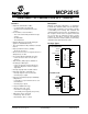
MCP2515 Stand-Alone CAN Controller With SPI™ Interface Features Description • Implements CAN V2.
MCP2515 NOTES: DS21801D-page 2 Preliminary © 2005 Microchip Technology Inc.
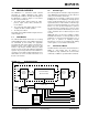
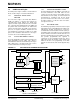
MCP2515 1.0 DEVICE OVERVIEW 1.2 The MCP2515 is a stand-alone CAN controller developed to simplify applications that require interfacing with a CAN bus. A simple block diagram of the MCP2515 is shown in Figure 1-1. The device consists of three main blocks: 1. The CAN module, which includes the CAN protocol engine, masks, filters, transmit and receive buffers. The control logic and registers that are used to configure the device and its operation. The SPI protocol block. 2. 3.
MCP2515 FIGURE 1-2: EXAMPLE SYSTEM IMPLEMENTATION Node Controller Node Controller Node Controller SPI SPI MCP2515 MCP2515 MCP2515 TX TX TX SPI™ RX XCVR RX RX XCVR XCVR CANH CANL TABLE 1-1: Name PINOUT DESCRIPTION PDIP/SOIC TSSOP Pin # Pin # I/O/P Type Description Alternate Pin Function TXCAN 1 1 O Transmit output pin to CAN bus — RXCAN 2 2 I Receive input pin from CAN bus — CLKOUT 3 3 O Clock output pin with programmable prescaler Start-of-Frame signal TX0RTS 4
MCP2515 1.4 Transmit/Receive Buffers/Masks/Filters The MCP2515 has three transmit and two receive buffers, two acceptance masks (one for each receive buffer) and a total of six acceptance filters. Figure 1-3 shows a block diagram of these buffers and their connection to the protocol engine.
MCP2515 1.5 1.5.3 CAN Protocol Engine The CAN protocol engine combines several functional blocks, shown in Figure 1-4 and described below. 1.5.1 PROTOCOL FINITE STATE MACHINE The heart of the engine is the Finite State Machine (FSM). The FSM is a sequencer that controls the sequential data stream between the TX/RX shift register, the CRC register and the bus line. The FSM also controls the Error Management Logic (EML) and the parallel data stream between the TX/RX shift registers and the buffers.
MCP2515 2.0 CAN MESSAGE FRAMES The MCP2515 supports standard data frames, extended data frames and remote frames (standard and extended), as defined in the CAN 2.0B specification. 2.1 Standard Data Frame The CAN standard data frame is shown in Figure 2-1. As with all other frames, the frame begins with a StartOf-Frame (SOF) bit, which is of the dominant state and allows hard synchronization of all nodes.
MCP2515 2.4.1 ACTIVE ERRORS 2.5 If an error-active node detects a bus error, the node interrupts transmission of the current message by generating an active error flag. The active error flag is composed of six consecutive dominant bits. This bit sequence actively violates the bit-stuffing rule. All other stations recognize the resulting bit-stuffing error and, in turn, generate error frames themselves, called error echo flags.
Start-of-Frame ID 10 0 Preliminary Stored in Buffers Message Filtering Identifier 11 12 Arbitration Field ID3 © 2005 Microchip Technology Inc.
Start-Of-Frame ID10 0 ID3 Preliminary Message Filtering Identifier 11 Stored in Buffers 11 18 Extended Identifier Arbitration Field ID0 SRR IDE EID17 000 Bit-stuffing 8 Stored in Transmit/Receive Buffers Data Length Code 4 8N (0 ≤ N ≤ 8) Data Field 8 Data Frame (number of bits = 64 + 8N) 6 Control Field EID0 RTR RB1 RB0 DLC3 DS21801D-page 10 Reserved bits CRC 15 16 CRC Field IFS 11111111111 CRC Del Ack Slot Bit ACK Del 1 End-ofFrame 7 FIGURE 2-2: DLC0 32 MCP2515 EXTENDED DATA
Start-Of-Frame ID10 Preliminary Message Filtering Identifier ID3 1 1 18 Extended Identifier Remote Frame with Extended Identifier 0 11 Arbitration Field ID0 SRR IDE EID17 © 2005 Microchip Technology Inc.
Start-Of-Frame ID 10 0 Message Filtering Identifier 11 ID3 12 Arbitration Field 6 Control Field 4 0 0 0 Preliminary Bit-stuffing Data Length Code ID0 RTR IDE RB0 DLC3 DS21801D-page 12 Reserved Bit 8 Data Frame or Remote Frame 8N (0≤N≤8) Data Field 8 Inter-Frame Space or Overload Frame 0 0 1 1 1 1 1 1 1 1 0 Error Delimiter Echo Error Flag Error Flag 0 0 0 0 0 0 0 8 £6 6 Error Frame FIGURE 2-4: DLC0 Interrupted Data Frame MCP2515 ACTIVE ERROR FRAME © 2005 Microchip Technology Inc.
© 2005 Microchip Technology Inc.
MCP2515 NOTES: DS21801D-page 14 Preliminary © 2005 Microchip Technology Inc.
MCP2515 3.0 MESSAGE TRANSMISSION 3.3 3.1 Transmit Buffers In order to initiate message transmission, the TXBnCTRL.TXREQ bit must be set for each buffer to be transmitted. This can be accomplished by: The MCP2515 implements three transmit buffers. Each of these buffers occupies 14 bytes of SRAM and are mapped into the device memory map. The first byte, TXBnCTRL, is a control register associated with the message buffer.
MCP2515 3.5 TXnRTS PINS 3.6 The TXnRTS pins are input pins that can be configured as: • Request-to-send inputs, which provides an alternative means of initiating the transmission of a message from any of the transmit buffers • Standard digital inputs Configuration and control of these pins is accomplished using the TXRTSCTRL register (see Register 3-2). The TXRTSCTRL register can only be modified when the MCP2515 is in Configuration mode (see Section 10.0 “Modes of Operation”).
MCP2515 FIGURE 3-1: TRANSMIT MESSAGE FLOWCHART Start The message transmission sequence begins when the device determines that the TXBnCTRL.TXREQ for any of the transmit registers has been set. Are any TXBnCTRL.TXREQ bits = 1 ? No Yes Clearing the TxBnCTRL.TXREQ bit while it is set, or setting the CANCTRL.ABAT bit before the message has started transmission, will abort the message. Clear: TXBnCTRL.ABTF TXBnCTRL.MLOA TXBnCTRL.TXERR Is CAN bus available to start transmission? No is TXBnCTRL.
MCP2515 REGISTER 3-1: TXBnCTRL – TRANSMIT BUFFER n CONTROL REGISTER (ADDRESS: 30h, 40h, 50h) U-0 R-0 R-0 R-0 R/W-0 U-0 R/W-0 R/W-0 — ABTF MLOA TXERR TXREQ — TXP1 TXP0 bit 7 bit 0 bit 7 Unimplemented: Read as ‘0’ bit 6 ABTF: Message Aborted Flag bit 1 = Message was aborted 0 = Message completed transmission successfully bit 5 MLOA: Message Lost Arbitration bit 1 = Message lost arbitration while being sent 0 = Message did not lose arbitration while being sent bit 4 TXERR: Transmissio
MCP2515 REGISTER 3-2: TXRTSCTRL – TXnRTS PIN CONTROL AND STATUS REGISTER (ADDRESS: 0Dh) U-0 U-0 R-x R-x R-x R/W-0 — — B2RTS B1RTS B0RTS B2RTSM R/W-0 R/W-0 B1RTSM B0RTSM bit 7 bit 0 bit 7 Unimplemented: Read as ‘0’ bit 6 Unimplemented: Read as ‘0’ bit 5 B2RTS: TX2RTS Pin State bit - Reads state of TX2RTS pin when in Digital Input mode - Reads as ‘0’ when pin is in ‘Request-to-Send’ mode bit 4 B1RTS: TX1RTX Pin State bit - Reads state of TX1RTS pin when in Digital Input mode - Reads a
MCP2515 REGISTER 3-4: TXBnSIDL – TRANSMIT BUFFER n STANDARD IDENTIFIER LOW (ADDRESS: 32h, 42h, 52h) R/W-x R/W-x R/W-x R/W-x R/W-x R/W-x R/W-x R/W-x SID2 SID1 SID0 — EXIDE — EID17 EID16 bit 7 bit 0 bit 7-5 SID: Standard Identifier bits <2:0> bit 4 Unimplemented: Reads as ‘0’ bit 3 EXIDE: Extended Identifier Enable bit 1 = Message will transmit extended identifier 0 = Message will transmit standard identifier bit 2 Unimplemented: Reads as ‘0’ bit 1-0 EID: Extended Identifier bits <
MCP2515 REGISTER 3-7: TXBnDLC - TRANSMIT BUFFER n DATA LENGTH CODE (ADDRESS: 35h, 45h, 55h) R/W-x R/W-x R/W-x R/W-x R/W-x R/W-x R/W-x R/W-x — RTR — — DLC3 DLC2 DLC1 DLC0 bit 7 bit 0 bit 7 Unimplemented: Reads as ‘0’ bit 6 RTR: Remote Transmission Request bit 1 = Transmitted Message will be a Remote Transmit Request 0 = Transmitted Message will be a Data Frame bit 5-4 Unimplemented: Reads as ‘0’ bit 3-0 DLC: Data Length Code <3:0> bits Sets the number of data bytes to be transmitted
MCP2515 NOTES: DS21801D-page 22 Preliminary © 2005 Microchip Technology Inc.
MCP2515 4.0 MESSAGE RECEPTION 4.1 Receive Message Buffering 4.2 The MCP2515 includes two full receive buffers with multiple acceptance filters for each. There is also a separate Message Assembly Buffer (MAB) that acts as a third receive buffer (see Figure 4-2). 4.1.1 MESSAGE ASSEMBLY BUFFER Of the three receive buffers, the MAB is always committed to receiving the next message from the bus. The MAB assembles all messages received.
MCP2515 4.3 4.4.1 Start-of-Frame Signal The RXBnBF pins can be disabled to the highimpedance state by clearing BFPCTRL.BnBFE. If enabled, the Start-Of-Frame signal is generated on the SOF pin at the beginning of each CAN message detected on the RXCAN pin. 4.4.2 The RXCAN pin monitors an idle bus for a recessiveto-dominant edge. If the dominant condition remains until the sample point, the MCP2515 interprets this as a SOF and a SOF pulse is generated.
MCP2515 4.4.3 CONFIGURED AS DIGITAL OUTPUT When used as digital outputs, the BFPCTRL.BxBFM bit must be cleared and BFPCTRL.BnBFE must be set for the associated buffer. In this mode, the state of the pin is controlled by the BFPCTRL.BnBFS bits. Writing a ‘1’ to the BnBFS bit will cause a high level to be driven on the associated buffer full pin, while a ‘0’ will cause the pin to drive low.
MCP2515 FIGURE 4-3: RECEIVE FLOW FLOWCHART Start Detect Start of Message? No Yes Begin Loading Message into Message Assembly Buffer (MAB) Generate Error Frame Valid Message Received? No Yes Yes Meets a filter criteria for RXB0? No Meets a filter criteria for RXB1? Yes No Go to Start Determines if the receive register is empty and able to accept a new message Determines if RXB0 can roll over into RXB1, if it is full. Is No CANINTF.RX0IF = 0? Is RXB0CTRL.
MCP2515 REGISTER 4-1: RXB0CTRL – RECEIVE BUFFER 0 CONTROL (ADDRESS: 60h) U-0 R/W-0 R/W-0 U-0 R-0 R/W-0 R-0 R-0 — RXM1 RXM0 — RXRTR BUKT BUKT1 FILHIT0 bit 7 bit 0 bit 7 Unimplemented: Read as ‘0’ bit 6-5 RXM: Receive Buffer Operating Mode bits 11 = Turn mask/filters off; receive any message 10 = Receive only valid messages with extended identifiers that meet filter criteria 01 = Receive only valid messages with standard identifiers that meet filter criteria 00 = Receive all valid messag
MCP2515 REGISTER 4-2: RXB1CTRL – RECEIVE BUFFER 1 CONTROL (ADDRESS: 70h) U-0 R/W-0 R/W-0 U-0 R-0 R-0 R-0 R-0 — RXM1 RXM0 — RXRTR FILHIT2 FILHIT1 FILHIT0 bit 7 bit 0 bit 7 Unimplemented: Read as ‘0’ bit 6-5 RXM: Receive Buffer Operating Mode bits 11 = Turn mask/filters off; receive any message 10 = Receive only valid messages with extended identifiers that meet filter criteria 01 = Receive only valid messages with standard identifiers that meet filter criteria 00 = Receive all valid mes
MCP2515 REGISTER 4-3: BFPCTRL – RXnBF PIN CONTROL AND STATUS (ADDRESS: 0Ch) U-0 U-0 R/W-0 R/W-0 R/W-0 R/W-0 R/W-0 R/W-0 — — B1BFS B0BFS B1BFE B0BFE B1BFM B0BFM bit 7 bit 0 bit 7 Unimplemented: Read as ‘0’ bit 6 Unimplemented: Read as ‘0’ bit 5 B1BFS: RX1BF Pin State bit (Digital Output mode only) - Reads as ‘0’ when RX1BF is configured as interrupt pin bit 4 B0BFS: RX0BF Pin State bit (Digital Output mode only) - Reads as ‘0’ when RX0BF is configured as interrupt pin bit 3 B1BFE:
MCP2515 REGISTER 4-5: RXBnSIDL – RECEIVE BUFFER n STANDARD IDENTIFIER LOW (ADDRESS: 62h, 72h) R-x R-x R-x R-x R-x U-0 R-x R-x SID2 SID1 SID0 SRR IDE — EID17 EID16 bit 7 bit 0 bit 7-5 SID: Standard Identifier bits <2:0> These bits contain the three least significant bits of the Standard Identifier for the received message bit 4 SRR: Standard Frame Remote Transmit Request bit (valid only if IDE bit = ‘0’) 1 = Standard Frame Remote Transmit Request Received 0 = Standard Data Frame Receive
MCP2515 REGISTER 4-7: RXBnEID0 – RECEIVE BUFFER n EXTENDED IDENTIFIER LOW (ADDRESS: 64h, 74h) R-x R-x R-x R-x R-x R-x R-x R-x EID7 EID6 EID5 EID4 EID3 EID2 EID1 EID0 bit 7 bit 7-0 bit 0 EID: Extended Identifier bits <7:0> These bits hold the least significant eight bits of the Extended Identifier for the received message Legend: REGISTER 4-8: R = Readable bit W = Writable bit U = Unimplemented bit, read as ‘0’ -n = Value at POR ‘1’ = Bit is set ‘0’ = Bit is cleared x = Bit is unkn
MCP2515 4.5 Message Acceptance Filters and Masks The message acceptance filters and masks are used to determine if a message in the message assembly buffer should be loaded into either of the receive buffers (see Figure 4-5). Once a valid message has been received into the MAB, the identifier fields of the message are compared to the filter values. If there is a match, that message will be loaded into the appropriate receive buffer. 4.5.
MCP2515 4.5.3 FILHIT BITS Filter matches on received messages can be determined by the FILHIT bits in the associated RXBnCTRL register. RXB0CTRL.FILHIT0 for buffer 0 and RXB1CTRL.FILHIT<2:0> for buffer 1.
MCP2515 REGISTER 4-10: RXFnSIDH – FILTER n STANDARD IDENTIFIER HIGH (ADDRESS: 00h, 04h, 08h, 10h, 14h, 18h) R/W-x R/W-x R/W-x R/W-x R/W-x R/W-x R/W-x R/W-x SID10 SID9 SID8 SID7 SID6 SID5 SID4 SID3 bit 7 bit 7-0 bit 0 SID: Standard Identifier Filter bits <10:3> These bits hold the filter bits to be applied to bits <10:3> of the Standard Identifier portion of a received message Legend: REGISTER 4-11: R = Readable bit W = Writable bit U = Unimplemented bit, read as ‘0’ -n = Value at POR
MCP2515 REGISTER 4-12: RXFnEID8 – FILTER n EXTENDED IDENTIFIER HIGH (ADDRESS: 02h, 06h, 0Ah, 12h, 16h, 1Ah) R/W-x R/W-x R/W-x R/W-x R/W-x R/W-x R/W-x R/W-x EID15 EID14 EID13 EID12 EID11 EID10 EID9 EID8 bit 7 bit 7-0 bit 0 EID: Extended Identifier bits <15:8> These bits hold the filter bits to be applied to bits <15:8> of the Extended Identifier portion of a received message Legend: REGISTER 4-13: R = Readable bit W = Writable bit U = Unimplemented bit, read as ‘0’ -n = Value at POR
MCP2515 REGISTER 4-15: RXMnSIDL – MASK n STANDARD IDENTIFIER LOW (ADDRESS: 21h, 25h) R/W-0 R/W-0 R/W-0 U-0 U-0 U-0 R/W-0 R/W-0 SID2 SID1 SID0 — — — EID17 EID16 bit 7 bit 0 bit 7-5 SID: Standard Identifier Mask bits <2:0> These bits hold the mask bits to be applied to bits<2:0> of the Standard Identifier portion of a received message bit 4-2 Unimplemented: Reads as ‘0’ bit 1-0 EID: Extended Identifier Mask bits <17:16> These bits hold the mask bits to be applied to bits <17:16> of the
MCP2515 5.0 BIT TIMING 5.1 All nodes on a given CAN bus must have the same nominal bit rate. The CAN protocol uses Non Return to Zero (NRZ) coding, which does not encode a clock within the data stream. Therefore, the receive clock must be recovered by the receiving nodes and synchronized to the transmitter’s clock.
MCP2515 PROPAGATION SEGMENT Therefore: The Propagation Segment (PropSeg) exists to compensate for physical delays between nodes. The propagation delay is defined as twice the sum of the signal’s propagation time on the bus line, including the delays associated with the bus driver. The PropSeg is programmable from 1 – 8 TQ. PHASE SEGMENT 1 (PS1) AND PHASE SEGMENT 2 (PS2) The two phase segments, PS1 and PS2, are used to compensate for edge phase errors on the bus.
MCP2515 5.2 5.2.2.2 Synchronization No Phase Error (e = 0) To compensate for phase shifts between the oscillator frequencies of each of the nodes on the bus, each CAN controller must be able to synchronize to the relevant signal edge of the incoming signal. Synchronization is the process by which the DPLL function is implemented. If the magnitude of the phase error is less than or equal to the programmed value of the SJW, the effect of a resynchronization is the same as that of a hard synchronization.
MCP2515 FIGURE 5-3: SYNCHRONIZING THE BIT TIME Input Signal (e = 0) PhaseSeg2 (PS2) PropSeg SyncSeg PhaseSeg1 (PS1) SJW (PS2) SJW (PS1) Sample Point Nominal Bit Time (NBT) No Resynchronization (e = 0) Input Signal (e > 0) PhaseSeg2 (PS2) SyncSeg PhaseSeg1 (PS1) PropSeg SJW (PS2) SJW (PS1) Sample Point Nominal Bit Time (NBT) Actual Bit Time Resynchronization to a Slower Transmitter (e > 0) Input Signal (e < 0) SyncSeg PropSeg PhaseSeg1 (PS1) PhaseSeg2 (PS2) SJW (PS2) SJW (PS1) Sample Point N
MCP2515 5.3 Programming Time Segments 5.5 Some requirements for programming of the time segments: • PropSeg + PS1 >= PS2 • PropSeg + PS1 >= TDELAY • PS2 > SJW For example, assuming that a 125 kHz CAN baud rate with FOSC = 20 MHz is desired: TOSC = 50 ns, choose BRP<5:0> = 04h, then TQ = 500 ns. To obtain 125 kHz, the bit time must be 16 TQ. Typically, the sampling of the bit should take place at about 60-70% of the bit time, depending on the system parameters. Also, typically, the TDELAY is 1-2 TQ.
MCP2515 REGISTER 5-1: CNF1 – CONFIGURATION 1 (ADDRESS: 2Ah) R/W-0 R/W-0 R/W-0 R/W-0 R/W-0 R/W-0 R/W-0 R/W-0 SJW1 SJW0 BRP5 BRP4 BRP3 BRP2 BRP1 BRP0 bit 7 bit 0 bit 7-6 SJW: Synchronization Jump Width Length bits <1:0> 11 = Length = 4 x TQ 10 = Length = 3 x TQ 01 = Length = 2 x TQ 00 = Length = 1 x TQ bit 5-0 BRP: Baud Rate Prescaler bits <5:0> TQ = 2 x (BRP + 1)/FOSC Legend: REGISTER 5-2: R = Readable bit W = Writable bit U = Unimplemented bit, read as ‘0’ -n = Value at POR ‘1’ =
MCP2515 REGISTER 5-3: CNF3 - CONFIGURATION 1 (ADDRESS: 28h) R/W-0 R/W-0 U-0 U-0 U-0 R/W-0 R/W-0 R/W-0 SOF WAKFIL — — — PHSEG22 PHSEG21 PHSEG20 bit 7 bit 0 bit 7 SOF: Start-of-Frame signal bit If CANCTRL.CLKEN = 1: 1 = CLKOUT pin enabled for SOF signal 0 = CLKOUT pin enabled for clockout function If CANCTRL.CLKEN = 0, Bit is don’t care.
MCP2515 NOTES: DS21801D-page 44 Preliminary © 2005 Microchip Technology Inc.
MCP2515 6.0 ERROR DETECTION 6.6 The CAN protocol provides sophisticated error detection mechanisms. The following errors can be detected. 6.1 CRC Error With the Cyclic Redundancy Check (CRC), the transmitter calculates special check bits for the bit sequence from the start of a frame until the end of the data field. This CRC sequence is transmitted in the CRC Field. The receiving node also calculates the CRC sequence using the same formula and performs a comparison to the received sequence.
MCP2515 FIGURE 6-1: ERROR MODES STATE DIAGRAM RESET Error-Active REC < 127 or TEC < 127 128 occurrences of 11 consecutive “recessive” bits REC > 127 or TEC > 127 Error-Passive TEC > 255 Bus-Off REGISTER 6-1: TEC – TRANSMIT ERROR COUNTER (ADDRESS: 1Ch) R-0 R-0 R-0 R-0 R-0 R-0 R-0 R-0 TEC7 TEC6 TEC5 TEC4 TEC3 TEC2 TEC1 TEC0 bit 7 bit 7-0 bit 0 TEC: Transmit Error Count bits <7:0> Legend: REGISTER 6-2: R = Readable bit W = Writable bit U = Unimplemented bit, read as ‘0’ -n = Valu
MCP2515 REGISTER 6-3: EFLG – ERROR FLAG (ADDRESS: 2Dh) R/W-0 R/W-0 R-0 R-0 R-0 R-0 R-0 R-0 RX1OVR RX0OVR TXBO TXEP RXEP TXWAR RXWAR EWARN bit 7 bit 0 bit 7 RX1OVR: Receive Buffer 1 Overflow Flag bit - Set when a valid message is received for RXB1 and CANINTF.RX1IF = 1 - Must be reset by MCU bit 6 RX0OVR: Receive Buffer 0 Overflow Flag bit - Set when a valid message is received for RXB0 and CANINTF.
MCP2515 NOTES: DS21801D-page 48 Preliminary © 2005 Microchip Technology Inc.
MCP2515 7.0 INTERRUPTS 7.2 Transmit Interrupt The MCP2515 has eight sources of interrupts. The CANINTE register contains the individual interrupt enable bits for each interrupt source. The CANINTF register contains the corresponding interrupt flag bit for each interrupt source. When an interrupt occurs, the INT pin is driven low by the MCP2515 and will remain low until the interrupt is cleared by the MCU. An interrupt can not be cleared if the respective condition still prevails.
MCP2515 7.6.2 RECEIVER WARNING 7.6.6 The REC has reached the MCU warning limit of 96. 7.6.3 The TEC has exceeded 255 and the device has gone to bus-off state. TRANSMITTER WARNING 7.7 The TEC has reached the MCU warning limit of 96. 7.6.4 Interrupt Acknowledge Interrupts are directly associated with one or more status flags in the CANINTF register. Interrupts are pending as long as one of the flags is set.
MCP2515 REGISTER 7-2: CANINTF – INTERRUPT FLAG (ADDRESS: 2Ch) R/W-0 R/W-0 R/W-0 R/W-0 R/W-0 R/W-0 R/W-0 R/W-0 MERRF WAKIF ERRIF TX2IF TX1IF TX0IF RX1IF RX0IF bit 7 bit 0 bit 7 MERRF: Message Error Interrupt Flag bit 1 = Interrupt pending (must be cleared by MCU to reset interrupt condition) 0 = No interrupt pending bit 6 WAKIF: Wakeup Interrupt Flag bit 1 = Interrupt pending (must be cleared by MCU to reset interrupt condition) 0 = No interrupt pending bit 5 ERRIF: Error Interrupt Fl
MCP2515 NOTES: DS21801D-page 52 Preliminary © 2005 Microchip Technology Inc.
MCP2515 8.0 OSCILLATOR 8.2 CLKOUT Pin The MCP2515 is designed to be operated with a crystal or ceramic resonator connected to the OSC1 and OSC2 pins. The MCP2515 oscillator design requires the use of a parallel cut crystal. Use of a series cut crystal may give a frequency out of the crystal manufacturers specifications. A typical oscillator circuit is shown in Figure 8-1. The MCP2515 may also be driven by an external clock source connected to the OSC1 pin, as shown in Figure 8-2 and Figure 8-3.
MCP2515 EXTERNAL SERIES RESONANT CRYSTAL OSCILLATOR CIRCUIT(1) FIGURE 8-3: 330 kΩ 330 kΩ 74AS04 74AS04 To Other Devices 74AS04 MCP2510 OSC1 0.1 mF XTAL Note 1: Duty cycle restrictions must be observed (see Table 12-2). TABLE 8-1: CAPACITOR SELECTION FOR CERAMIC RESONATORS TABLE 8-2: CAPACITOR SELECTION FOR CRYSTAL OSCILLATOR Typical Capacitor Values Used: Mode Freq. OSC1 OSC2 HS 8.0 MHz 27 pF 27 pF 16.
MCP2515 9.0 RESET The MCP2515 differentiates between two resets: 1. 2. Hardware Reset – Low on RESET pin. SPI Reset – Reset via SPI command. Both of these resets are functionally equivalent. It is important to provide one of these two resets after power-up to ensure that the logic and registers are in their default state. A hardware reset can be achieved automatically by placing an RC on the RESET pin. (see Figure 9-1).
MCP2515 NOTES: DS21801D-page 56 Preliminary © 2005 Microchip Technology Inc.
MCP2515 10.0 MODES OF OPERATION The MCP2515 has five modes of operation. These modes are: 1. 2. 3. 4. 5. Configuration mode. Normal mode. Sleep mode. Listen-only mode. Loopback mode. The operational mode is selected via CANCTRL. REQOP bits (see Register 10-1). The TXCAN pin will remain in the recessive state while the MCP2515 is in Sleep mode. 10.2.1 the When changing modes, the mode will not actually change until all pending message transmissions are complete.
MCP2515 10.4 Loopback Mode 10.5 Loopback mode will allow internal transmission of messages from the transmit buffers to the receive buffers without actually transmitting messages on the CAN bus. This mode can be used in system development and testing. Normal Mode Normal mode is the standard operating mode of the MCP2515. In this mode, the device actively monitors all bus messages and generates acknowledge bits, error frames, etc.
MCP2515 REGISTER 10-2: CANSTAT – CAN STATUS REGISTER (ADDRESS: XEh) R-1 R-0 R-0 OPMOD2 OPMOD1 OPMOD0 U-0 R-0 R-0 R-0 U-0 — ICOD2 ICOD1 ICOD0 — bit 7 bit 0 bit 7-5 OPMOD: Operation Mode bits <2:0> 000 = Device is in the Normal operation mode 001 = Device is in Sleep mode 010 = Device is in Loopback mode 011 = Device is in Listen-only mode 100 = Device is in Configuration mode bit 4 Unimplemented: Read as ‘0’ bit 3-1 ICOD: Interrupt Flag Code bits <2:0> 000 = No Interrupt 001 = Error Int
MCP2515 NOTES: DS21801D-page 60 Preliminary © 2005 Microchip Technology Inc.
MCP2515 11.0 REGISTER MAP reading and writing of data. Some specific control and status registers allow individual bit modification using the SPI Bit Modify command. The registers that allow this command are shown as shaded locations in Table 11-1. A summary of the MCP2515 control registers is shown in Table 11-2. The register map for the MCP2515 is shown in Table 11-1. Address locations for each register are determined by using the column (higher-order 4 bits) and row (lower-order 4 bits) values.
MCP2515 NOTES: DS21801D-page 62 Preliminary © 2005 Microchip Technology Inc.
MCP2515 12.0 SPI™ INTERFACE 12.1 Overview The MCP2515 is designed to interface directly with the Serial Peripheral Interface (SPI) port available on many microcontrollers and supports Mode 0,0 and Mode 1,1. Commands and data are sent to the device via the SI pin, with data being clocked in on the rising edge of SCK. Data is driven out by the MCP2515 (on the SO line) on the falling edge of SCK. The CS pin must be held low while any operation is performed.
MCP2515 Each status bit returned in this command may also be read by using the standard read command with the appropriate register address. The part is selected by lowering the CS pin and the Bit Modify command byte is then sent to the MCP2515. The command is followed by the address of the register, the mask byte and finally the data byte. 12.9 The mask byte determines which bits in the register will be allowed to change.
MCP2515 FIGURE 12-2: READ INSTRUCTION CS 0 1 2 3 4 5 6 7 8 9 10 11 12 13 14 15 16 17 18 19 20 21 22 23 SCK instruction 0 SI 0 0 0 address byte 0 0 1 A7 1 6 5 4 3 2 1 A0 don’t care data out high-impedance 7 SO FIGURE 12-3: 6 5 4 3 2 1 0 READ RX BUFFER INSTRUCTION CS n m 0 1 2 3 4 5 6 7 8 9 10 11 12 13 14 15 SCK instruction SI 1 0 0 1 0 n m 0 don’t care data out high-impedance 7 SO FIGURE 12-4: 6 5 4 3 2 1 0 Address Points to Address 0
MCP2515 FIGURE 12-5: LOAD TX BUFFER a b c CS 0 1 2 3 4 5 6 7 8 9 10 11 12 13 14 15 SCK data in instruction SI 0 1 0 0 0 a b c 7 6 5 4 3 2 1 0 high-impedance SO FIGURE 12-6: Address Points to Addr 0 0 0 TX buffer 0, Start at TXB0SIDH 0x31 0 0 1 TX buffer 0, Start at TXB0D0 0x36 0 1 0 TX buffer 1, Start at TXB1SIDH 0x41 0 1 1 TX buffer 1, Start at TXB1D0 0x46 1 0 0 TX buffer 2, Start at TXB2SIDH 0x51 1 0 1 TX buffer 2, Start at TXB2D0 0x56 REQUEST-TO-SEND (RTS) IN
MCP2515 FIGURE 12-8: READ STATUS INSTRUCTION CS 0 1 2 3 4 5 6 7 8 9 10 11 12 13 14 15 16 17 18 19 20 21 22 23 SCK instruction SI 1 0 1 0 0 0 0 don’t care 0 repeat data out data out high-impedance 7 SO 6 5 4 3 2 1 0 7 6 5 4 3 2 1 0 CANINTF.RX0IF CANINTFL.RX1IF TXB0CNTRL.TXREQ CANINTF.TX0IF TXB1CNTRL.TXREQ CANINTF.TX1IF TXB2CNTRL.TXREQ CANINTF.
MCP2515 FIGURE 12-10: SPI™ INPUT TIMING 3 CS 11 10 6 1 7 Mode 1,1 SCK 2 Mode 0,0 4 5 SI MSB in LSB in high-impedance SO FIGURE 12-11: SPI™ OUTPUT TIMING CS 8 2 9 SCK Mode 1,1 Mode 0,0 12 13 SO SI DS21801D-page 68 MSB out 14 LSB out don’t care Preliminary © 2005 Microchip Technology Inc.
MCP2515 13.0 ELECTRICAL CHARACTERISTICS 13.1 Absolute Maximum Ratings † VDD.............................................................................................................................................................................7.0V All inputs and outputs w.r.t. VSS ..........................................................................................................-0.6V to VDD +1.0V Storage temperature ............................................................................
MCP2515 TABLE 13-1: DC CHARACTERISTICS Industrial (I): Extended (E): DC Characteristics Param. No. Sym Characteristic TAMB = -40°C to +85°C TAMB = -40°C to +125°C Min Max Units VDD = 2.7V to 5.5V VDD = 4.5V to 5.5V Conditions VDD Supply Voltage 2.7 5.5 V VRET Register Retention Voltage 2.4 — V 2 VDD + 1 V SCK, CS, SI, TXnRTS Pins 0.7 VDD VDD + 1 V OSC1 0.85 VDD VDD V RESET 0.85 VDD VDD V RXCAN, TXnRTS Pins -0.3 .15 VDD V SCK, CS, SI -0.3 0.4 V OSC1 VSS .
MCP2515 TABLE 13-2: OSCILLATOR TIMING CHARACTERISTICS Oscillator Timing Characteristics(Note) Param. No. Note: Sym Characteristic Min Max Units VDD = 2.7V to 5.5V VDD = 4.5V to 5.5V Conditions Clock-In Frequency 1 1 40 25 MHz MHz 4.5V to 5.5V 2.7V to 5.5V TOSC Clock-In Period 25 40 1000 1000 ns ns 4.5V to 5.5V 2.7V to 5.5V TDUTY Duty Cycle (External Clock Input) 0.45 0.55 — TOSH/(TOSH + TOSL) This parameter is periodically sampled and not 100% tested.
MCP2515 TABLE 13-5: CLKOUT PIN AC CHARACTERISTICS CLKOUT Pin AC/DC Characteristics Param. No. Sym Characteristic Industrial (I): Extended (E): TAMB = -40°C to +85°C TAMB = -40°C to +125°C Min Max Units VDD = 2.7V to 5.5V VDD = 4.5V to 5.5V Conditions thCLKOUT CLKOUT Pin High Time 15 — ns TOSC = 40 ns (Note 1) tlCLKOUT CLKOUT Pin Low Time 15 — ns TOSC = 40 ns (Note 1) trCLKOUT CLKOUT Pin Rise Time — 5 ns Measured from 0.3 VDD to 0.
MCP2515 TABLE 13-6: SPI™ INTERFACE AC CHARACTERISTICS SPI™ Interface AC Characteristics Param. No.
MCP2515 NOTES: DS21801D-page 74 Preliminary © 2005 Microchip Technology Inc.
MCP2515 14.0 PACKAGING INFORMATION 14.1 Package Marking Information 18-Lead PDIP (300 mil) Example: MCP2515-I/P^^ e3 XXXXXXXXXXXXXXXXX XXXXXXXXXXXXXXXXX YYWWNNN 0434256 18-Lead SOIC (300 mil) Example: XXXXXXXXXXXX XXXXXXXXXXXX XXXXXXXXXXXX YYWWNNN MCP2515 E/SO^^ e3 0434256 20-Lead TSSOP (4.4 mm) Example: XXXXXXXX MCP2515 XXXXXNNN IST e^3 256 YYWW 0434 Legend: XX...
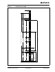
MCP2515 18-Lead Plastic Dual In-line (P) – 300 mil (PDIP) E1 D 2 n α 1 E A2 A L c A1 B1 β p B eB Units Dimension Limits n p MIN INCHES* NOM 18 .100 .155 .130 MAX MILLIMETERS NOM 18 2.54 3.56 3.94 2.92 3.30 0.38 7.62 7.94 6.10 6.35 22.61 22.80 3.18 3.30 0.20 0.29 1.14 1.46 0.36 0.46 7.87 9.40 5 10 5 10 MIN Number of Pins Pitch Top to Seating Plane A .140 .170 Molded Package Thickness A2 .115 .145 Base to Seating Plane A1 .015 Shoulder to Shoulder Width E .300 .313 .
MCP2515 18-Lead Plastic Small Outline (SO) – Wide, 300 mil (SOIC) E p E1 D 2 B n 1 h α 45° c A2 A φ β L Units Dimension Limits n p Number of Pins Pitch Overall Height Molded Package Thickness Standoff § Overall Width Molded Package Width Overall Length Chamfer Distance Foot Length Foot Angle Lead Thickness Lead Width Mold Draft Angle Top Mold Draft Angle Bottom A A2 A1 E E1 D h L φ c B α β MIN .093 .088 .004 .394 .291 .446 .010 .016 0 .009 .014 0 0 A1 INCHES* NOM 18 .050 .099 .091 .
MCP2515 20-Lead Plastic Thin Shrink Small Outline (ST) – 4.4 mm (TSSOP) E p E1 D B 2 n 1 α A c φ β L Units Dimension Limits n p Number of Pins Pitch Overall Height Molded Package Thickness Standoff § Overall Width Molded Package Width Molded Package Length Foot Length Foot Angle Lead Thickness Lead Width Mold Draft Angle Top Mold Draft Angle Bottom A A2 A1 E E1 D L φ c B α β MIN .033 .002 .246 .169 .252 .020 0 .004 .007 0 0 A2 A1 INCHES NOM 20 .026 .035 .004 .251 .173 .256 .024 4 .006 .
MCP2515 APPENDIX A: REVISION HISTORY Revision D (April 2005) The following is the list of modifications: 1. 2. 3. 4. Section 8.0. Added Table 8-1 and Table 8-2. Added note box following tables. Section 11.0, Table 11-1. Changed address bits in column heading. Modified Section 14.0 Packaging Information to reflect pb free device markings. Appendix A Revision History: Rearranged order of importance. Revision C (November 2004) The following is the list of modifications: 1. 2. 3. New section 9.0 added.
MCP2515 NOTES: DS21801D-page 80 Preliminary © 2005 Microchip Technology Inc.
MCP2515 PRODUCT IDENTIFICATION SYSTEM To order or obtain information, e.g., on pricing or delivery, refer to the factory or the listed sales office. PART NO.
MCP2515 NOTES: DS21801D-page 82 Preliminary © 2005 Microchip Technology Inc.
Note the following details of the code protection feature on Microchip devices: • Microchip products meet the specification contained in their particular Microchip Data Sheet. • Microchip believes that its family of products is one of the most secure families of its kind on the market today, when used in the intended manner and under normal conditions. • There are dishonest and possibly illegal methods used to breach the code protection feature.
WORLDWIDE SALES AND SERVICE AMERICAS ASIA/PACIFIC ASIA/PACIFIC EUROPE Corporate Office 2355 West Chandler Blvd. Chandler, AZ 85224-6199 Tel: 480-792-7200 Fax: 480-792-7277 Technical Support: http://support.microchip.com Web Address: www.microchip.