
Parallax P2 Edge Module - Datasheet
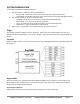
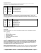
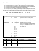
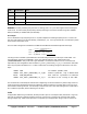
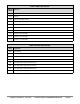
Table Of Contents
- FEATURES
- HARDWARE
- Pin Descriptions
- Hardware Connections
- Minimal Connections
- External Crystal
- Reset Switch
- SPI Flash Boot Memory
- MicroSD Boot Memory
- Dual Boot Memory
- OPERATION
- SYSTEM ORGANIZATION
- Cogs
- Cog RAM
- Register RAM
- Lookup RAM
- Execution
- Hub
- Hub RAM
- Cog-to-Hub RAM Interface
- System Clock
- CORDIC Solver
- Smart I/O Pins
- Pin Modes
- I/O Pin Circuit
- Equivalent Schematics
- Smart Modes
- PASM2 LANGUAGE IN BRIEF
- Math and Logic
- Pin & Smart Pin
- Branch
- Hub Control, FIFO, & RAM
- Event
- Interrupt
- Register Indirection
- CORDIC Solver
- Color Space Converter and Pixel Mixer
- Lookup Table, Streamer, and Misc
- SYSTEM CHARACTERISTICS
- Absolute Maximum Electrical Ratings
- DC Characteristics
- AC Characteristics
- PACKAGING
- CHANGE LOG
- PARALLAX INCORPORATED

Dual-purpose Registers
RAM registers $1F0 through $1F7 may either be used as general-purpose registers, or may be used as
special-purpose registers if their associated functions are enabled.
Address
Name
Purpose
$1F0
$1F1
$1F2
$1F3
$1F4
$1F5
$1F6
$1F7
RAM / IJMP3
RAM / IRET3
RAM / IJMP2
RAM / IRET2
RAM / IJMP1
RAM / IRET1
RAM / PA
RAM / PB
Interrupt call address for INT3
Interrupt return address for INT3
Interrupt call address for INT2
Interrupt return address for INT2
Interrupt call address for INT1
Interrupt return address for INT1
CALLD-imm return, CALLPA parameter, or LOC address
CALLD-imm return, CALLPB parameter, or LOC address
Special-purpose Registers
RAM registers $1F8 through $1FF give mapped access to eight special-purpose functions. In general, when
specifying an address between $1F8 and $1FF, the PASM instruction accesses a special-purpose register, not just
the underlying RAM.
Address
Name
Purpose
$1F8
$1F9
$1FA
$1FB
$1FC
$1FD
$1FE
$1FF
PTRA
PTRB
DIRA
DIRB
OUTA
OUTB
INA
1
INB
2
Pointer A to Hub RAM
Pointer B to Hub RAM
Output enables for P31..P0
Output enables for P63..P32
Output states for P31..P0
Output states for P63..P32
Input states for P31..P0
Input states for P63..P32
1
Also debug interrupt call address
2
Also debug interrupt return address
Lookup RAM
Each cog's secondary 512 x 32-bit dual-port Lookup RAM (LUT RAM for short) is read and written as longs (4
bytes). It is useful for:
● Scratch space
● Streamer access
● Bytecode execution lookup table
● Smart pin data source
● Paired-Cog communication mechanism
● Code execution
Scratch Space
In contrast to Register RAM, the cog cannot directly reference Lookup RAM locations in the majority of its PASM
instructions. Instead, the desired location(s) must be read or written between Lookup RAM and Register RAM
using the RDLUT and WRLUT instructions, respectively. This is synonymous with other hardware architecture's
scratch storage using "LOAD" and "STORE" instructions. When using the RDLUT and WRLUT instructions, the
Lookup RAM's locations $200..$3FF are addressable as $000..$1FF.
Paired-Cog Communication Mechanism
Adjacent cogs whose ID numbers differ by only the LSB (cogs 0 and 1, 2 and 3, etc.) can allow their Lookup RAMs
to be written by the other cog via its local Lookup RAM writes. This allows adjacent cogs to share data quickly
Copyright © Parallax Inc. 2021/05/27 ▪ Parallax Propeller 2 (P2X8C4M64P) Datasheet ▪ Page 12