
User's Manual


PMAC2 VME Hardware Reference Manual
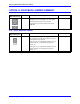
Jumper Summary 29
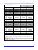
98 GND Common Reference Voltage
99 +5V Output / Input +5v Power For external circuit or from external supply
100 +5V Output / Input +5v Power
The JMACH3 connector provides the interface pins for channels 5 and 6. It is usually connected to a breakout board, such
as one of the Acc-8x family of boards, or an application-specific interface board.
Note: 100-pin male box header with center key, 0050 pitch. AMP part # 1-04068-7.
Delta Tau part # 014-00010-FPB.
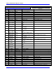
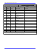
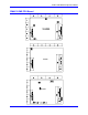
J12/JMACH4 (100-Pin Header)
1
2
99
1
00
Front View
Pin# Symbol Function Description Notes
1 +5V Output / Input +5V Power For external circuit or from external supply
2 +5V Output / Input +5V Power
3 GND Common Reference Voltage
4 GND Common Reference Voltage
5 CHA7+ Input Enc 7 Pos. A Chan. Also pulse input
6 CHA7- Input Enc 7 Neg. A Chan.
7 CHB7+ Input Enc 7 Pos. B Chan. Also direction input
8 CHB7- Input Enc 7 Neg. B Chan.
9 CHC7+ Input Enc 7 Pos. C Chan. Index channel
10 CHC7- Input Enc 7 Neg. C Chan.
11 CHU7 Input Chan 7 U Flag Hall effect, fault code, or sub-count
12 CHV7 Input Chan 7 V Flag Hall effect, fault code, or sub-count
13 CHW7 Input Chan 7 W Flag Hall effect, fault code, or sub-count
14 CHT7 Input Chan 7 T Flag Fault code, or sub-count
15 USER7 Input General Purpose User Flag Hardware capture flag, or sub-count
16 PLIM7 Input Positive Overtravel Limit Hardware capture flag
17 MLIM7 Input Negative Overtravel Limit Hardware capture flag
18 HOME7 Input Home Switch Input Hardware capture flag
19 ACCFLT7 Input Accessory Fault Flag For loss of ACC supply voltage
20 WD0/ Output Watchdog Output Low is PMAC watchdog fault
21 SCLK78+ Input / Output Encoder Sample Clock Direction controlled by PMAC2 jumper
22 SCLK78- Input / Output Encoder Sample Clock
23 ADC_CLK7+ Output A/D Converter Clock Programmable frequency
24 ADC_CLK7- Output A/D Converter Clock
25 ADC_STB7+ Output A/D Converter Strobe Programmable sequence
26 ADC_STB7- Output A/D Converter Strobe
27 ADC_DAA7+ Input Chan A ADC Serial Data MSB first
28 ADC_DAA7- Input Chan A ADC Serial Data
29 ADC_DAB7+ Input Chan B ADC Serial Data MSB first
30 ADC_DAB7- Input Chan B ADC Serial Data
31 AENA7+ Output Amplifier Enable High is enable
32 AENA7- Output Amplifier Enable Low is enable
33 FAULT7+ Input Amplifier Fault Programmable polarity
34 FAULT7- Input Amplifier Fault
35 PWMATOP7+
DAC_CLK7+
Output Phase A Top CMD or DAC
Clock
Programmable function control
36 PWMATOP7-
DAC_CLK7-
Output Phase A Top CMD or DAC
Clock
37 PWMABOT7+
DAC7A+
Output Phase A Bottom CMD or DAC
A Serial Data
Programmable function control
38 PWMABOT7-
DAC7A-
Output Phase A Bottom CMD or DAC
A Serial Data