
User's Manual

PMAC VME Hardware Reference Manual
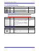
26 Jumper Summary
Option 1V Piggyback Connector Description
The following paragraphs provide a brief description of each connector on the Option 1V Piggyback card,
its use, and individual pinout information (see Figure 2-2).
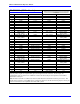
P17
J11
J12
E14
JP1
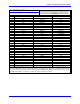
2222222PP2222PP2222PP222
P2
1-1
1-16
1-8
1-24
1-4
1-20
1-13
1-28
1-3
1-18
1-10
1-26
1-6
1-22
1-14
1-30
1-2
1-17
1-9
1-25
1-5
1-21
1-12
1-29
1-19
1-11
1-27
1-7
1-23
1-15
1-31
1-32
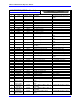
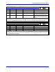
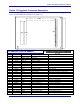
J11/JMACH3 (100-Pin Header)
1
2
99
1
00
Front View
Pin# Symbol Function Description Notes
1 +5V Output / Input +5V Power For external circuit or from external supply
2 +5V Output / Input +5V Power
3 GND Common Reference Voltage
4 GND Common Reference Voltage
5 CHA5+ Input Enc 5 Pos. A Chan. Also pulse input
6 CHA5- Input Enc 5 Neg. A Chan.
7 CHB5+ Input Enc 5 Pos. B Chan. Also direction input
8 CHB5- Input Enc 5 Neg. B Chan.
9 CHC5+ Input Enc 5 Pos. C Chan. Index channel
10 CHC5- Input Enc 5 Neg. C Chan.
11 CHU5 Input Chan 5 U Flag Hall effect, fault code, or sub-count
12 CHV5 Input Chan 5 V Flag Hall effect, fault code, or sub-count
13 CHW5 Input Chan 5 W Flag Hall effect, fault code, or sub-count
14 CHT5 Input Chan 5 T Flag Fault code, or sub-count
15 USER5 Input General Purpose User Flag Hardware capture flag, or sub-count
16 PLIM5 Input Positive Overtravel Limit Hardware capture flag
17 MLIM5 Input Negative Overtravel Limit Hardware capture flag
18 HOME5 Input Home Switch Input Hardware capture flag
19 ACCFLT5 Input Accessory Fault Flag For loss of acc supply voltage
20 WD0/ Output Watchdog Output Low is PMAC Watchdog Fault
21 SCLK56+ Input / Output Encoder Sample Clock Direction controlled by PMAC2 jumper
22 SCLK56- Input / Output Encoder Sample Clock
23 ADC_CLK5+ Output A/D Converter Clock Programmable frequency
24 ADC_CLK5- Output A/D Converter Clock