
Reference Manual
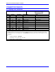
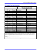
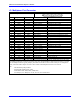
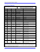
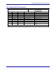
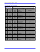

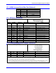
Table Of Contents
- Base Version
- Option 2: Dual-Ported RAM
- Option 5xF: CPU Speed Options
- Option 6: Extended Servo Algorithm Firmware
- Option 6L: Special Lookahead Firmware
- Option 10: Firmware Version Specification
- Option 12: Analog-to-Digital Converters
- Option 15: V-to-F Converter for Analog Input
- Option 16: Battery-Backed Parameter Memory
- Digital Power Supply
- Analog Power Supply
- Resistor Pack Configuration: Flag and Digital Inputs Voltage Selection
- Types of Overtravel Limits
- Home Switches
- Incremental Encoder Connection
- DAC Output Signals
- Amplifier Enable Signal (AENAx/DIRn)
- Amplifier Fault Signal (FAULTn)
- Command Inputs
- Selector Inputs
- Alternate Use
- Reset Input
- Handwheel Inputs
- Optional Voltage to Frequency Converter
- J1 - Display Port (JDISP Port)
- J2 - Control-Panel Port (JPAN Port)
- J3 - Thumbwheel Multiplexer Port (JTHW Port)
- J4 - Serial Port (JRS422 Port)
- J5 - General-Purpose Digital Inputs and Outputs (JOPTO Port)
- J6 – Expansion Port \(JXIO Port\)
- J8 - Machine Connectors (JMACH Port)
- J9 – Compare Equal Outputs Port \(JEQU Port\)
- J17 - Serial Port (JRS232 Port)
- J30 – Optional Analog to Digital Inputs \(JANA P
- J31 – Optional Universal Serial Bus Port \(JUSB
- JS1 – Expansion Ports \(JS1 Port\)
- TB1 – Power Supply Terminal Block \(JPWR Connect
- LED Indicators
- Fuse
- J1 (JDISP)/Display
- J2 (JPAN)/Control Panel
- J3 (JTHW)/Multiplexer Port
- J4 (JRS422)/RS232 OR 422/Serial Communications
- J5 (JOPT)/OPTO I/O
- J6 (JXIO)/Expansion Board
- J8 (JMACH)/Machine Connector
- JS1/A-D Inputs 1-4
- JEQU/Position Compare
- JANA/Analog Inputs Option
PMAC PCI-Lite Hardware Reference Manual
54 Connector Pinouts
J31 (JUSB) Universal Serial Bus Port (Optional)
Pin # Symbol Function
1 VCC N.C.
2 D- Data-
3 D+ Data+
4 GND GND
5 Shell Shield
6 Shell Shield
JS1: A/D Port 1 Connector
JS1 (16-Pin Header)
Front View
Pin # Symbol Function Description Notes
1 DCLK Output D to A, A to D Clock DAC and ADC clock for chan 1,
2, 3, 4
2 BDATA1 Output D to A Data DAC data for chan 1, 2, 3, 4
3 ASEL0/ Output Chan Select Bit 0 Select for chan 1, 2, 3, 4
4 ASEL1/ Output Chan Select Bit 1 Select for chan 1, 2, 3, 4
5 CNVRT01 Output A to D Convert ADC convert sig. Chan 1, 2, 3, 4
6 ADCIN1 Input A to D Data ADC data for chan 1, 2, 3, 4
7 OUT1/ Output Amp Enable/Dir Amp enable/dir. for chan 1
8 OUT2/ Output Amp Enable/Dir Amp enable/dir. for chan 2
9 OUT3/ Output Amp Enable/Dir Amp enable/dir. for chan 3
10 OUT4/ Output Amp Enable/Dir Amp enable/dir. for chan 4
11 HF41 Input Amp Fault Amp fault input for chan 1
12 HF42 Input Amp Fault Amp fault input for chan 2
13 HF43 Input Amp Fault Amp fault input for chan 3
14 HF44 Input Amp Fault Amp fault input for chan 4
15 +5V Output +5v Supply Power supply out
16 GND Common PMAC Common
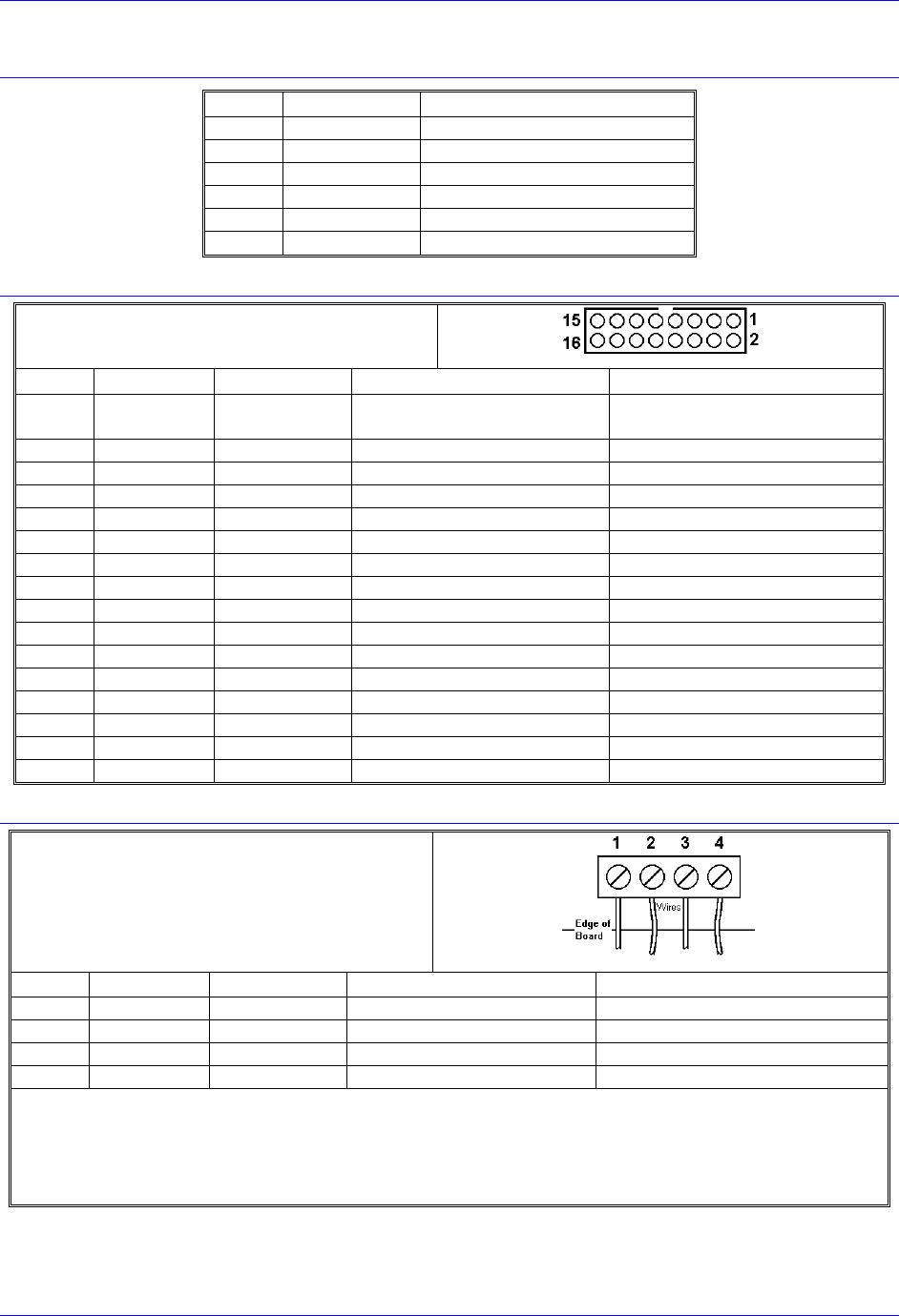
TB1 (JPWR) External Power Supply Connection
TB1 (JPWR)
Top View
Pin # Symbol Function Description Notes
1 GND Common Digital ground
2 +5V Input +5v supply Ref. to digital GND
3 +12V Input +12v to +15v supply Ref. to digital GND
4 -12V Input -12v to -15v supply Ref. to digital GND
This terminal block may be used as an alternative power supply connector if PMAC is not installed in a PCI-
bus. The +5V powers the digital electronics. The +12V and -12V (if jumpers E85, E87, and E88 are installed)
power the analog output stage. This defeats the optical isolation on PMAC.
To keep the optical isolation between the digital and analog circuits on PMAC, provide analog power (+/-12V
to +/-15V and AGND) through the JMACH connector instead of the bus connector or this terminal block.