
Reference Manual
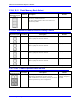
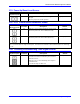
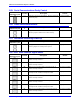
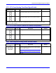
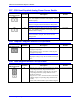
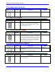

Table Of Contents
- Base Version
- Option 2: Dual-Ported RAM
- Option 5xF: CPU Speed Options
- Option 6: Extended Servo Algorithm Firmware
- Option 6L: Special Lookahead Firmware
- Option 10: Firmware Version Specification
- Option 12: Analog-to-Digital Converters
- Option 15: V-to-F Converter for Analog Input
- Option 16: Battery-Backed Parameter Memory
- Digital Power Supply
- Analog Power Supply
- Resistor Pack Configuration: Flag and Digital Inputs Voltage Selection
- Types of Overtravel Limits
- Home Switches
- Incremental Encoder Connection
- DAC Output Signals
- Amplifier Enable Signal (AENAx/DIRn)
- Amplifier Fault Signal (FAULTn)
- Command Inputs
- Selector Inputs
- Alternate Use
- Reset Input
- Handwheel Inputs
- Optional Voltage to Frequency Converter
- J1 - Display Port (JDISP Port)
- J2 - Control-Panel Port (JPAN Port)
- J3 - Thumbwheel Multiplexer Port (JTHW Port)
- J4 - Serial Port (JRS422 Port)
- J5 - General-Purpose Digital Inputs and Outputs (JOPTO Port)
- J6 – Expansion Port \(JXIO Port\)
- J8 - Machine Connectors (JMACH Port)
- J9 – Compare Equal Outputs Port \(JEQU Port\)
- J17 - Serial Port (JRS232 Port)
- J30 – Optional Analog to Digital Inputs \(JANA P
- J31 – Optional Universal Serial Bus Port \(JUSB
- JS1 – Expansion Ports \(JS1 Port\)
- TB1 – Power Supply Terminal Block \(JPWR Connect
- LED Indicators
- Fuse
- J1 (JDISP)/Display
- J2 (JPAN)/Control Panel
- J3 (JTHW)/Multiplexer Port
- J4 (JRS422)/RS232 OR 422/Serial Communications
- J5 (JOPT)/OPTO I/O
- J6 (JXIO)/Expansion Board
- J8 (JMACH)/Machine Connector
- JS1/A-D Inputs 1-4
- JEQU/Position Compare
- JANA/Analog Inputs Option
PMAC PCI Lite Hardware Reference Manual
E-Point Jumper Descriptions 35
E29 - E33: Phase Clock Frequency Control
Jumpers E29 through E33 control the speed of the phase clock, and, indirectly, the servo clock, which is
divided down from the phase clock (see E3 - E6). No more than one of these five jumpers may be on at a
time.
Phase Clock Frequency
E29 E30 E31 E32 E33
E98 Connects
Pins 1 and 2
E98 Connects
Pins 2 and 3
Default and
Physical
Layout
Location
On Off Off Off Off 2.26 kHz 1.13 kHz
E29
A8
Off On Off Off Off 4.52 kHz 2.26 kHz
E30
A8
Off Off On Off Off 9.04 kHz 4.52 kHz
E31
A8
Off Off Off On Off 18.07 kHz 9.04 kHz
E32
A8
Off Off Off Off On 36.14 kHz 18.07 kHz
E33
A8
Note: If E40-E43 are not all ON, the phase clock is received from an external source through the J4 serial-
port connector, and the settings of E29 – E33 are not relevant.
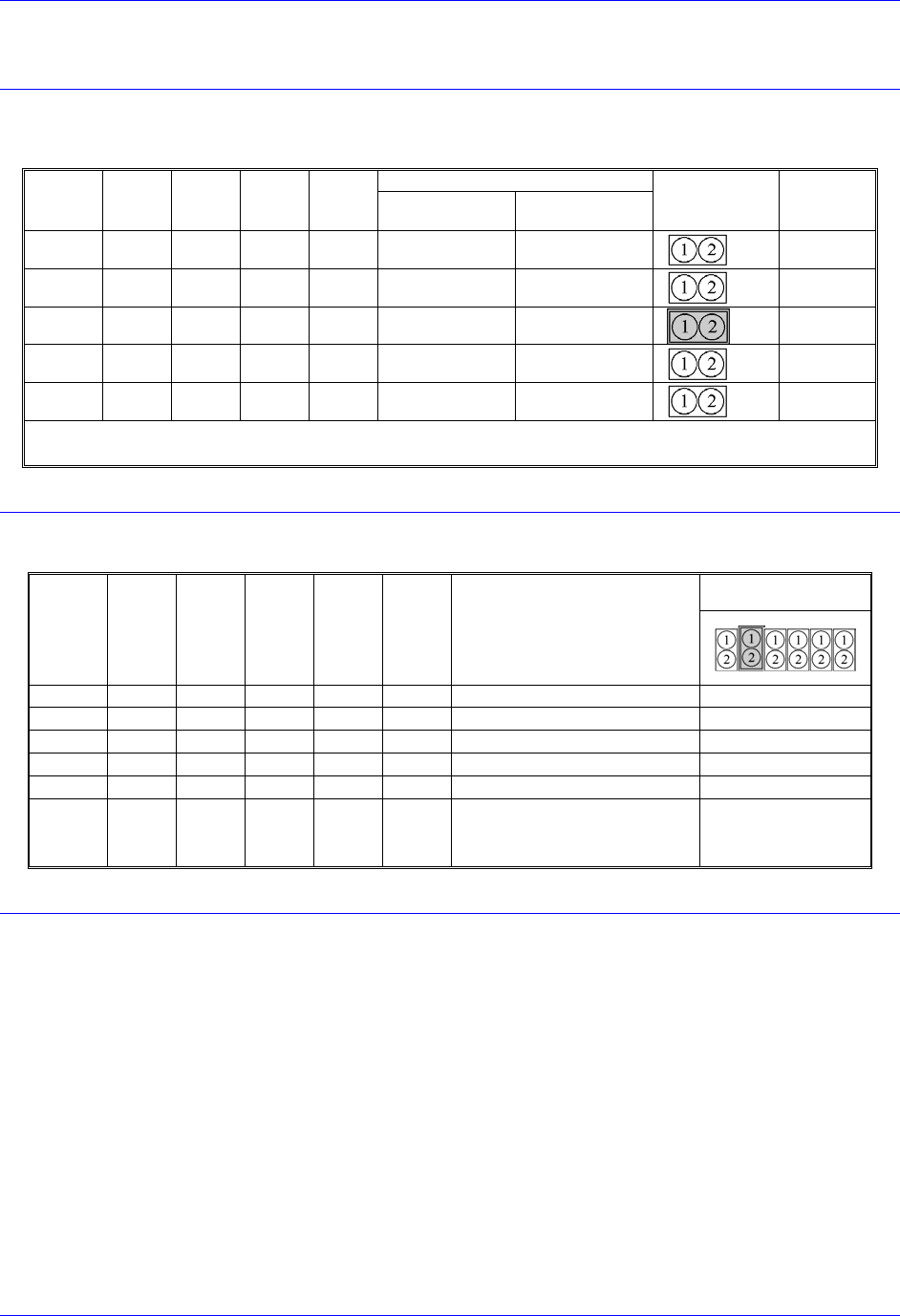
E34A - E38: Encoder Sampling Clock Frequency Control
Jumpers E34A - E38 control the encoder-sampling clock (SCLK) used by the gate array ICs. No more
than one of these six jumpers may be on at a time.
Default and Physical
Layout
E34A E34 E35 E36 E37 E38 SCLK Clock Frequency
E34A E34 E35 E36 E37 E38
A8 A8 A8 A8 A8 A8
On Off Off Off Off Off 19.6608 MHz
Off On Off Off Off Off 9.8304 MHz E34 ON
Off Off On Off Off Off 4.9152 MHz
Off Off Off On Off Off 2.4576 MHz
Off Off Off Off On Off 1.2288 MHz
Off Off Off Off Off On External Clock 1 to 30MHz
maximum input on CHC4 &
CHC4/
E40 - E43: Clock Direction Control
Jumpers E40 – E43 determine the direction of the phase and servo clocks. All of these jumpers must be
ON for the card to use its internally generated clock signals and to output these on the serial port
connector. If any of these jumpers is OFF, the card will expect to input these clock signals from the serial
port connector, and its watchdog timer will trip immediately if it does not receive these signals. The card
number (0 – 15) for serial addressing of multiple cards on a daisy chain serial cable is determined by the
PMAC variable I0.
See the Software Setup section in this manual for details.