
Reference Manual
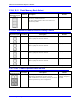
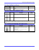
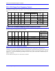
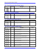
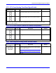
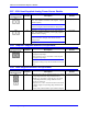
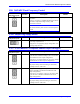
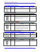

Table Of Contents
- Base Version
- Option 2: Dual-Ported RAM
- Option 5xF: CPU Speed Options
- Option 6: Extended Servo Algorithm Firmware
- Option 6L: Special Lookahead Firmware
- Option 10: Firmware Version Specification
- Option 12: Analog-to-Digital Converters
- Option 15: V-to-F Converter for Analog Input
- Option 16: Battery-Backed Parameter Memory
- Digital Power Supply
- Analog Power Supply
- Resistor Pack Configuration: Flag and Digital Inputs Voltage Selection
- Types of Overtravel Limits
- Home Switches
- Incremental Encoder Connection
- DAC Output Signals
- Amplifier Enable Signal (AENAx/DIRn)
- Amplifier Fault Signal (FAULTn)
- Command Inputs
- Selector Inputs
- Alternate Use
- Reset Input
- Handwheel Inputs
- Optional Voltage to Frequency Converter
- J1 - Display Port (JDISP Port)
- J2 - Control-Panel Port (JPAN Port)
- J3 - Thumbwheel Multiplexer Port (JTHW Port)
- J4 - Serial Port (JRS422 Port)
- J5 - General-Purpose Digital Inputs and Outputs (JOPTO Port)
- J6 – Expansion Port \(JXIO Port\)
- J8 - Machine Connectors (JMACH Port)
- J9 – Compare Equal Outputs Port \(JEQU Port\)
- J17 - Serial Port (JRS232 Port)
- J30 – Optional Analog to Digital Inputs \(JANA P
- J31 – Optional Universal Serial Bus Port \(JUSB
- JS1 – Expansion Ports \(JS1 Port\)
- TB1 – Power Supply Terminal Block \(JPWR Connect
- LED Indicators
- Fuse
- J1 (JDISP)/Display
- J2 (JPAN)/Control Panel
- J3 (JTHW)/Multiplexer Port
- J4 (JRS422)/RS232 OR 422/Serial Communications
- J5 (JOPT)/OPTO I/O
- J6 (JXIO)/Expansion Board
- J8 (JMACH)/Machine Connector
- JS1/A-D Inputs 1-4
- JEQU/Position Compare
- JANA/Analog Inputs Option
PMAC PCI Lite Hardware Reference Manual
E-Point Jumper Descriptions 33
E10A, B, C: Flash Memory Bank Select
E Point and
Physical Layout
Location Description Default
E10A
E10C
A2 &B2 Remove all three jumpers to select flash memory bank
with factory-installed firmware.
Use other configurations to select one of the seven
flash memory banks.
No jumpers installed
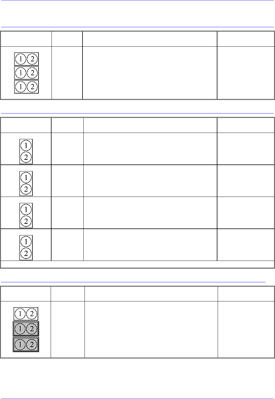
E17A-D: Amplifier Enable/Direction Polarity Control
E Point and
Physical Layout
Location Description Default
E17A
A8 Jump 1-2 for high-true AENA1.
Remove jumper for low-true AENA1.
No jumper installed
E17B
A8 Jump 1-2 for high-true AENA2.
Remove jumper for low-true AENA2.
No jumper installed
E17C
A8 Jump 1-2 for high-true AENA3.
Remove jumper for low-true AENA3.
No jumper installed
E17D
A7 Jump 1-2 for high-true AENA4.
Remove jumper for low-true AENA4.
No jumper installed
Note: Low-true enable is the fail-safe option because of the sinking (open-collector) ULN2803A output driver IC.
E18 – E20: Power-Up/Reset Load Source
E Point and
Physical Layout
Location Description Default
E18
E20
B4 Remove jumper E18. Jump E19.
Jump E20 to read flash IC on power-up/reset.
Other combinations are for factory use only; the board
will not operate in any other configuration.
No E18 jumper
installed. Jump E19
and E20.