
Reference Manual


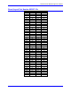

Table Of Contents
- Base Version
- Option 2: Dual-Ported RAM
- Option 5xF: CPU Speed Options
- Option 6: Extended Servo Algorithm Firmware
- Option 6L: Special Lookahead Firmware
- Option 10: Firmware Version Specification
- Option 12: Analog-to-Digital Converters
- Option 15: V-to-F Converter for Analog Input
- Option 16: Battery-Backed Parameter Memory
- Digital Power Supply
- Analog Power Supply
- Resistor Pack Configuration: Flag and Digital Inputs Voltage Selection
- Types of Overtravel Limits
- Home Switches
- Incremental Encoder Connection
- DAC Output Signals
- Amplifier Enable Signal (AENAx/DIRn)
- Amplifier Fault Signal (FAULTn)
- Command Inputs
- Selector Inputs
- Alternate Use
- Reset Input
- Handwheel Inputs
- Optional Voltage to Frequency Converter
- J1 - Display Port (JDISP Port)
- J2 - Control-Panel Port (JPAN Port)
- J3 - Thumbwheel Multiplexer Port (JTHW Port)
- J4 - Serial Port (JRS422 Port)
- J5 - General-Purpose Digital Inputs and Outputs (JOPTO Port)
- J6 – Expansion Port \(JXIO Port\)
- J8 - Machine Connectors (JMACH Port)
- J9 – Compare Equal Outputs Port \(JEQU Port\)
- J17 - Serial Port (JRS232 Port)
- J30 – Optional Analog to Digital Inputs \(JANA P
- J31 – Optional Universal Serial Bus Port \(JUSB
- JS1 – Expansion Ports \(JS1 Port\)
- TB1 – Power Supply Terminal Block \(JPWR Connect
- LED Indicators
- Fuse
- J1 (JDISP)/Display
- J2 (JPAN)/Control Panel
- J3 (JTHW)/Multiplexer Port
- J4 (JRS422)/RS232 OR 422/Serial Communications
- J5 (JOPT)/OPTO I/O
- J6 (JXIO)/Expansion Board
- J8 (JMACH)/Machine Connector
- JS1/A-D Inputs 1-4
- JEQU/Position Compare
- JANA/Analog Inputs Option
PMAC PCI-Lite Hardware Reference Manual
32 E-Point Jumper Descriptions
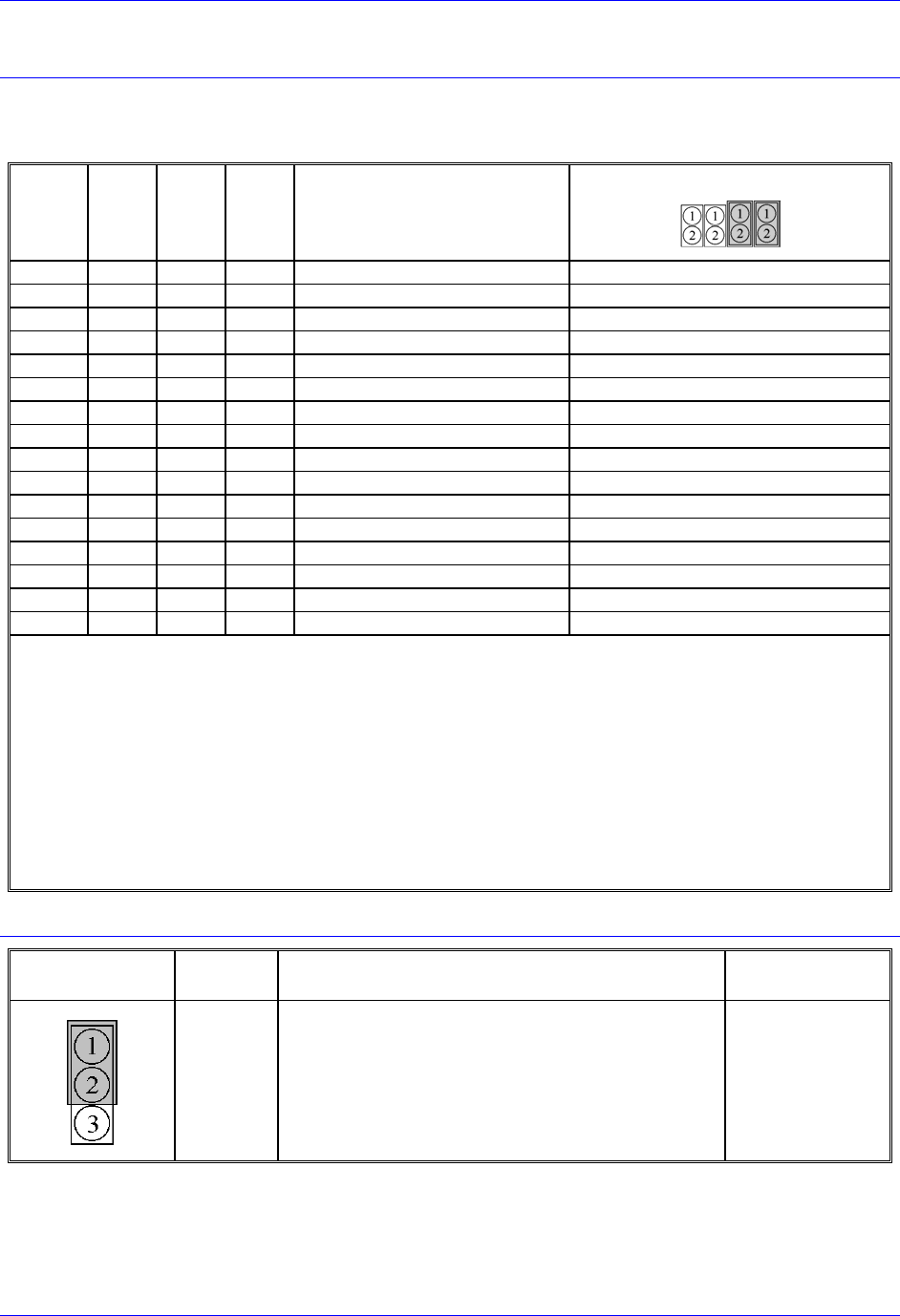
E3 - E6: Servo Clock Frequency Control
The servo clock (which determines how often the servo loop is closed) is derived from the phase clock
(see E98, E29 - E33) through a divide-by-N counter. Jumpers E3 through E6 control this dividing
function.
E3
E4
E5
E6
Servo Clock = Phase Clock
Divided by N
Default and Physical Layout
E3 E4 E5 E6
Location A8 A8 A8 A8
On On On On N = divided by 1
Off On On On N = divided by 2
On Off On On N = divided by 3
Off Off On On N = divided by 4 Only E5 and E6 ON
On Off On On N = divided by 5
Off On Off On N = divided by 6
On Off Off On N = divided by 7
Off Off Off On N = divided by 8
On On On Off N = divided by 9
Off On On Off N = divided by 10
On Off On Off N = divided by 11
Off Off On Off N = divided by 12
On On Off Off N = divided by 13
Off On Off Off N = divided by 14
On Off Off Off N = divided by 15
Off Off Off Off N = divided by 16
Note: Adjust the setting of I-variable I10 to match the servo interrupt cycle time set by E98, E3 – E6, E29 –
E33, and the crystal clock frequency. I10 holds the length of a servo interrupt cycle, scaled so that 8,388,608
equals one millisecond. Since I10 has a maximum value of 8,388,607, the servo interrupt cycle time should
always be less than a millisecond (unless the basic unit of time on PMAC should be something other than a
millisecond). To have a servo sample time greater than one millisecond, the sampling may be slowed in the
software with variable Ix60.
Frequency can be checked on J4 pins 21 & 22. It can also be checked from the software by typing RX:0 in the
PMAC terminal at 10-second intervals and dividing the difference of successive responses by 10000. The
resulting number is the approximate Servo Clock frequency kHz.
Note: If E40-E43 are not all ON, the phase clock is received from an external source through the J4 serial-port
connector, and the settings of E3 – E6 are not relevant.
E7: Machine Input Source/Sink Control
E Point and
Physical Layout
Location Description Default
E7
A6 Jump pin 1 to 2 to apply +5V to input reference resistor
SIP pack; this will bias MI1 to MI8 inputs to +5V for
OFF state; then input must be grounded for ON state.
Jump pin 2 to 3 to apply GND to input reference
resistor SIP pack; this will bias MI1 to MI8 inputs to
GND for OFF state; then input must be pulled up for
ON state (+5V to +24V).
1-2 Jumper
installed