
Reference Manual

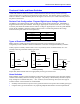
Table Of Contents
- Base Version
- Option 2: Dual-Ported RAM
- Option 5xF: CPU Speed Options
- Option 6: Extended Servo Algorithm Firmware
- Option 6L: Special Lookahead Firmware
- Option 10: Firmware Version Specification
- Option 12: Analog-to-Digital Converters
- Option 15: V-to-F Converter for Analog Input
- Option 16: Battery-Backed Parameter Memory
- Digital Power Supply
- Analog Power Supply
- Resistor Pack Configuration: Flag and Digital Inputs Voltage Selection
- Types of Overtravel Limits
- Home Switches
- Incremental Encoder Connection
- DAC Output Signals
- Amplifier Enable Signal (AENAx/DIRn)
- Amplifier Fault Signal (FAULTn)
- Command Inputs
- Selector Inputs
- Alternate Use
- Reset Input
- Handwheel Inputs
- Optional Voltage to Frequency Converter
- J1 - Display Port (JDISP Port)
- J2 - Control-Panel Port (JPAN Port)
- J3 - Thumbwheel Multiplexer Port (JTHW Port)
- J4 - Serial Port (JRS422 Port)
- J5 - General-Purpose Digital Inputs and Outputs (JOPTO Port)
- J6 – Expansion Port \(JXIO Port\)
- J8 - Machine Connectors (JMACH Port)
- J9 – Compare Equal Outputs Port \(JEQU Port\)
- J17 - Serial Port (JRS232 Port)
- J30 – Optional Analog to Digital Inputs \(JANA P
- J31 – Optional Universal Serial Bus Port \(JUSB
- JS1 – Expansion Ports \(JS1 Port\)
- TB1 – Power Supply Terminal Block \(JPWR Connect
- LED Indicators
- Fuse
- J1 (JDISP)/Display
- J2 (JPAN)/Control Panel
- J3 (JTHW)/Multiplexer Port
- J4 (JRS422)/RS232 OR 422/Serial Communications
- J5 (JOPT)/OPTO I/O
- J6 (JXIO)/Expansion Board
- J8 (JMACH)/Machine Connector
- JS1/A-D Inputs 1-4
- JEQU/Position Compare
- JANA/Analog Inputs Option
PMAC PCI Lite Hardware Reference Manual
Hardware Setup 7
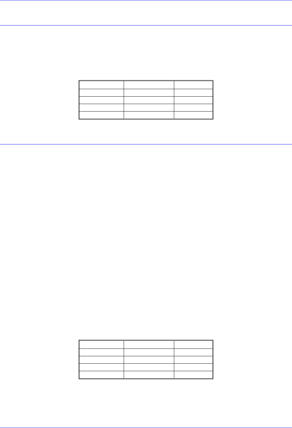
Resistor Pack Configuration: Termination Resistors
The PMAC provides sockets for termination resistors on differential input pairs coming into the board.
There are no resistor packs in these sockets when shipped. If these signals are brought long distances into
the PMAC board and ringing at signal transitions is a problem, SIP resistor packs may be mounted in
these sockets to reduce or eliminate the ringing.
All termination resistor packs have independent resistors (no common connection) with each resistor
using two adjacent pins. The following table shows which packs are used to terminate each input device:
Device Resistor Pack Pack Size
Encoder 1 RP61 6-pin
Encoder 2 RP63 6-pin
Encoder 3 RP67 6-pin
Encoder 4 RP69 6-pin
Resistor Pack Configuration: Differential or Single-Ended Encoder
Selection
The differential input signal pairs to the PMAC have user-configurable pull-up/pull-down resistor
networks to permit the acceptance of either single-ended or differential signals in one setting, or the
detection of lost differential signals in another setting.
• The ‘+’ inputs of each differential pair each have a hard-wired 1 kΩ pull-up resistor to +5V. This
cannot be changed.
• The ‘-’ inputs of each differential pair each have a hard-wired 2.2 kΩ resistor to +5V; also each has
another 2.2 kΩ resistor as part of a socketed resistor pack that can be configured as a pull-up resistor
to +5V, or a pull-down resistor to GND.
If this socketed resistor is configured as a pull-down resistor (the default configuration), the combination
of pull-up and pull-down resistors on this line acts as a voltage divider, holding the line at +2.5V in the
absence of an external signal. This configuration is required for single-ended inputs using the ‘+’ lines
alone; it is desirable for unconnected inputs to prevent the pick-up of spurious noise; it is permissible for
differential line-driver inputs.
If this socketed resistor is configured as a pull-up resistor (by reversing the SIP pack in the socket), the
two parallel 2.2 kΩ resistors act as a single 1.1 kΩ pull-up resistor, holding the line at +5V in the absence
of an external signal. This configuration is required if encoder-loss detection is desired; it is required if
complementary open-collector drivers are used; it is permissible for differential line-driver inputs even
without encoder loss detection.
If Pin 1 of the resistor pack (marked by a dot on the pack) matches Pin 1 of the socket (marked by a wide
white square solder pin on the front side of the board), then the pack is configured as a bank of pull-down
resistors. If the pack is reversed in the socket, it is configured as a bank of pull-up resistors.
The following table lists the pull-up/pull-down resistor pack for each input device:
Device Resistor Pack Pack Size
Encoder 1 RP60 6-pin
Encoder 2 RP62 6-pin
Encoder 3 RP66 6-pin
Encoder 4 RP68 6-pin