
Reference Manual


Mini PMAC Hardware Reference Manual
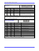
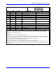
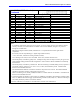
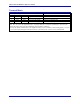
44 Schematics
int_vccio
GND
HREQ-
CS02-
irdy#
C96
0.1 mfd
-12V
tck_pci
EQU_2
18.07Khz
9.8304Mhz
MI1
VCC
HDB06
int_vccio
ad11
ad19
4.53Khz
aselx2
s2
SA7
BA10_A
par
HDB03
serr#
R13
200.0
1%
irdy#
SA11
E5
BA01_A
ad15
int_ground
BD09_A
BD07_A
R/WL-
2.4576Mhz
+
C78
68 mfd
25V
-
mini - PMAC1, PCI AND DUAL PORT RAM
Delta Tau Data Systems, Inc.
D
36Tuesday, May 07, 2002
603712-320
Title
Size Document Number Rev
Date: Sheet
of
RESET
BRD_A-
PHASE
VMECS-
idsel
c/be#1
SD7
bus_+5V
9.8304Mhz
TP5
A-14V
+5V
A+14V
devsel#
trst#
tms_pci
ad6
ad31
+12V
+5V
BD01_A
BD13_A
data0
HDB15
(ON HEATSINK)
int_vccio
+5V
BD15_A
E33
GND
GND
HDB14
SA9
19.6608Mhz
RESET
clock/phaseb
E6
+5V
A+5V
ad23
bus_gnd
+
C82
10 mfd tant/ceramic
16V
(TANT)
EQU_3
ad30
BUSYL-
E31
GND
SA9
AGND
18.07Khz
E35
+
C85
22 mfd
35V
E4
E36
C67
0.22 mfd
+
C77
10 mfd tant/ceramic
35V
(TANT)
VR3LM1117MPX-ADJ
MC33269ST-ADJ
(SOT-223)
3
1
2
IN
GND
OUT
BD08_A
BWR_A-
HDB01
ad14
int_ground
HDB09
BD04_A
BD05_A
SA0
BD05_A
R28
1K
R70
10K
ad2
BD07_A
VMECS-
C91
1 mfd
50V
JOIN GND, INT_GROUND
RAISE RESISTOR OFF BOARD
int_vccio
BD00_A
par
HDB08
SERVO
WDTC
C59
0.22 mfd
+5V
int_vccio
HDB07
SERVO
OEL-
WDO
HDB02
+12V
BX/Y_A
INIT-
WDTC
BA02_A
tdi_pci
ad26
ad24
BD02_A
s0
BSA04
C68
0.22 mfd
nstatus
ad0
UBL-
BUSYR-
SD6
s1
CEL-
D5
1SMC18AT3
R12 10k
-11V
trdy#
ad6
SD5
L1
56uh
+5V
HDB05
BA02_A
HDB04
SD4
SA1
BD23_A
ad[0..31]
ad26
EQU_1
HDB02
BSA04
INT_GROUND FROM C13 PIN 2
ad23
PWR
BD03_A
19.6608Mhz
BD05_A
BSA11
D2
1SMC15.0AT3
GND
SRD-
ad8
ad30
BD00_A
SCLK
bus_-12V
C53
0.22 mfd
int_vccint
nce
HDB00
ad27
BSA00
ASEL0
R22
1k
int_vccio
BA08_A
+12V
+5V
GND
HDB09
ad1
BD11_A
GND
bus_gnd
tdo_pci
ad12
ad3
BD00_A
led_rst
C66
0.22 mfd
+5V
BD11_A
tck_pci
tdi_pci
ad29
ad17
BSA02
1.2288Mhz
R28A
1K
SD5
ad1
ad7
ad16
RP11
10KSIP10C
1 2
3
4
5
6
7
8
910
D9A
LED
GRN
SA0
EQU_1
frame#
c/be#2
BD08_A
PHASE
R7
100
TP4
AGND
SA6
c/be#[0..3]
BSA05
SD1
ad3
ad22
SA5
rst#
E88
-12V
AGND
BA11_A
aselx2
C60
0.22 mfd
OR
int_vccio
SD3
HEN-
c/be#0
led_rst
TP2
A+14V
D10
LED
RED
A-14V
GND
BSA00
BD01_A
-11V
+5V
SD7
BD07_A
c/be#3
ad20
BD03_A
BD18_A
s0
BSA03
C62
0.1 mfd
+5V
idsel
ad11
BSA09
E85
VR5
LM7805T
(TO-220)
1
2
3
IN
GND
OUT
ad18
s1
C73
0.22 mfd
E37
C95
0.1 mfd
E85
BA11_A
ad10
HDB03
ASEL1
R27A
1K
R27
1K
R6
47k
VR4LM1117MPX-ADJ
MC33269ST-ADJ
(SOT-223)
3
1
2
IN
GND
OUT
SA3
SA8
ad24
HDB11
BSA02
C72
0.1 mfd
int_vccio
GND
CLKOUTR
SD4
HDB07
tdo_pci
SA14
D6
1SMC5.0AT3
+
C94
22 mfd
25V
GND
OEL-
IRQB-
MI1
int_vccint
GND
GND
ad28
HDB14
OPT 2
GND
GND
BSA00
BD07_A
BD00_A
PHASE
U22
epc1
1
2
3
4 5
6
7
8
data
dclk
oe
ncs gnd
ncasc
vcc
vcc
C57
0.22 mfd
WITH COPPER PAD
GND
DCLK
PHASE
ad5
BD17_A
GND
BD18_A
BD10_A
ad19
clock/phaseb
R19
121.0
1%
+5V
HDB01
SA2
-12V
BSA10
BD06_A
ODCLK
odflt
4.7 mfd tant
C79
"AGND" PLANE
vcc
+12V
ad21
BD02_A
E30
C86
0.01 mfd
WAIT1-
DPRBSY-
clk
R/WL-
+
C90
22 mfd
25V
U21
10k30eqc240 / 10k50eqc240
1
2
3
4
5
6
7
8
9
10
11
12
13
14
15
16
17
18
19
20
21
22
23
24
25
26
27
28
29
30
31
32
33
34
35
36
37
38
39
40
41
42
43
44
45
46
47
48
49
50
51
52
53
54
55
56
57
58
59
60
61
62
63
64
65
66
67
68
69
70
71
72
73
74
75
77
76
78
79
80
81
82
83
84
85
86
87
88
89
90
91
92
93
94
95
96
97
98
99
100
101
102
103
104
105
106
107
108
109
110
111
112
113
114
115
116
117
118
119
120
121
122
123
124
125
126
127
128
129
130
131
132
133
134
135
136
137
138
139
140
141
142
143
144
145
146
147
148
149
150
151
152
153
154
155
156
157
158
159
160
161
162
163
164
165
166
167
168
169
170
171
172
173
174
175
176
177
178
179
180
181
182
183
184
185
186
187
188
189
190
191
192
193
194
195
196
197
198
199
200
201
202
203
204
205
206
207
208
209
210
211
212
213
214
215
216
217
218
219
220
221
222
223
224
225
226
227
228
229
230
231
232
233
234
235
236
237
238
239
240
tck
conf_done
nceo
tdo
vccint
io
io
io
io
gndint
clkusr
io
io
io
io
vccio
io
io
io
io
io
gndint
rdynbsy
io
io
init_done
vccint
io
io
io
io
gndint
io
io
io
io
vccio
io
io
io
io
gndint
io
io
io
io
vccint
io
io
io
io
gndint
io
io
io
io
vccio
tms
trst
nstatus
io
io
io
io
io
io
io
io
gndint
io
io
io
io
io
io
vccio
io
io
io
io
io
io
io
io
gndint
io
io
io
vccint
in
ded. clk
in
gndint
io
io
vccint
io
io
io
io
io
io
io
gndint
io
io
io
io
io
io
io
vccio
io
io
io
io
io
io
io
io
nconfig
vccint
msel1
msel0
gndint
io
io
io
io
vccint
io
io
io
io
gndint
io
io
io
io
vccio
io
io
io
io
gndint
io
io
io
io
vccint
io
io
io
io
gndint
io
io
io
io
vccio
io
io
io
io
gndint
io
io
io
io
vccint
io
io
io
io
io
gndint
tdi
nce
dclk
d0
d0/io
d1/io
d3/io
io
d4/io
d5/io
io
d6/io
vccio
d7/io
io
io
io
io
io
io
gndint
io
io
io
io
io
io
io
vccio
io
io
io
dev_clrn
in
ded. clk
in
dev_oe
io
io
gndint
io
io
io
io
io
io
io
vccio
io
io
io
io
io
io
io
gndint
io
io
io
nrs
io
nws
cs
ncs
BD15_A
rst#
BSA13
2.26Khz
int_ground
BD12_A
BD05_A
SD2
SA6
BD13_A
WD
SA1
ad7
9.035Khz
R25
1k
R8
1k
E98
JUMPER3
2
3
1
C71
0.1 mfd
0.2 mfd ceramic per each power
ground pair
SERVO
c/be#1
HDB00
BD02_A
BD21_A
1.2288Mhz
+5V
BD10_A
WDO
BA07_A
2.26Khz
BSA01
P1
pcibus_connector
a58
b58
a57
b56
a55
b55
a54
b53
b52
a49
b48
a47
b47
a46
b45
a44
a32
b32
a31
b30
a29
b29
a28
b27
a25
b24
a23
b23
a22
b21
a20
b20
a52
b44
b33
b26
a43
a34
a36
b35
a38
b37
a26
b39
b40
b42
b16
a15
a6
b7
a7
b8
b18
a17
b11
b9
b2
a4
b4
a3
a1
a40
a41
a60
b60
b1
a2
b5
a5
b6
a8
a10
a16
b19
b3
b12
a12
b13
a13
b15
b17
a18
b22
a24
a30
b28
b34
a35
a37
b38
a42
b46
b49
b57
a48
a56
a61
b61
a62
b62
ad0
ad1
ad2
ad3
ad4
ad5
ad6
ad7
ad8
ad9
ad10
ad11
ad12
ad13
ad14
ad15
ad16
ad17
ad18
ad19
ad20
ad21
ad22
ad23
ad24
ad25
ad26
ad27
ad28
ad29
ad30
ad31
c/be#0
c/be#1
c/be#2
c/be#3
par
frame#
trdy#
irdy#
stop
devsel#
idsel
lock#
perr#
serr#
clk
rst#
inta#
intb#
intc#
intd#
req#
gnt#
prsnt2#
prsnt1#
tck
tdi
tdo
tms
trst#
sdone
sbo#
req64#
ack64#
-12V
+12V
+5V
+5V
+5V
+5V
+5V
+5V
+5V
gnd
gnd
gnd
gnd
gnd
gnd
gnd
gnd
gnd
gnd
gnd
gnd
gnd
gnd
gnd
gnd
gnd
gnd
gnd
gnd
gnd
gnd
+5V
+5V
+5V
+5V
int_vccio
+5V
GND
A+15V
AGND
BSA02
ad21
C74
0.22 mfd
C65
0.22 mfd
+
C76
4.7 mfd tant
16V
(TANT)
"DGND" PLANE
SD2
SA15
BA00_A
inta#
ad31
ad20
HDB13
BD19_A
BD03_A
BSA06
+5V
SA13
R9
10k
R21
1k
(JPWR)
+5V
SCLK
c/be#2
ad4
ad28
HDB05
BSA01
19.6608Mhz
SHOULD JOIN "GND" NET AT
THIS POINT
int_vccint
+5V
+11V
ODCLK
BA01_A
SA10
SA15
D7
1SMC18AT3
E34A
GND
+5V
c/be#3
int_vccint
CEL-
GND
VCC
SA11
+5V
BD09_A
nconfig
HDB04
ad10
ASEL0
UBL-
E87
BA05_A
c/be#3
BA00_A
C52
1.0 mfd
+
C84
68 mfd
25V
needs to be inverted for use with the phase/servo generator
int_vccint
EQU_1
BD12_A
L3
56uh
BD14_A
BD23_A
ASEL0
int_vccio
BSA08
R71
10K
OR
bus_-12V
BD06_A
data0
devsel#
ad0
ad18
+5V
IPOS
trdy#
HDB10
SA8
BD20_A
R10
1k
U19
NC7SZ14M5
2
3
4
5
2
3
4
5
L2
56uh
BD19_A
WDO
BUSYL-
+
C81
4.7 mfd tant
16V
(TANT)
R17
121.0
1%
+11V
-12V
SD0
c/be#2
c/be#0
ad4
BSA13
D3
1SMC15.0AT3
JP1
SOLDER JUMPER
E29
SA5
BUSYR-
s3
C83
0.1 mfd
SD0
SA4
BD06_A
BD09_A
R18
1k
U18
NC7SZ14M5
2
3
4
5
2
3
4
5
+5V
BD04_A
c/be#1
ad15
+5V
HR/W-
BD17_A
BD20_A
EQU_2
nce
ad27
BD01_A
E3
AGND
HDB05
c/be#[0..3]
ad9
C56
0.22 mfd
R16
1k
C75
0.22 mfd
PWR
HOSTINT
BD02_A
tms_pci
DPRCS-
R11
1k
+
C93
22 mfd
35V
U20
CY7C025-TQFP
(TQFP100)
11
10
8
7
6
5
100
99
98
97
96
95
94
93
91
90
82
81
80
79
78
77
76
71
70
69
68
67
66
87
84
83
85
89
64
86
65
35
33
32
31
30
29
28
27
26
21
20
19
18
16
15
14
43
44
45
46
47
48
49
50
55
56
57
58
59
37
41
42
40
36
61
39
60
62
38
34
9
13
63
92
88
17
12
I/O-15L
I/O-14L
I/O-13L
I/O-12L
I/O-11L
I/O-10L
I/O-09L
I/O-08L
I/O-07L
I/O-06L
I/O-05L
I/O-04L
I/O-03L
I/O-02L
I/O-01L
I/O-00L
A12L
A11L
A10L
A09L
A08L
A07L
A06L
A05L
A04L
A03L
A02L
A01L
A00L
R/WL
UBL
LBL
CEL
OEL
BUSYL
SEML
INTL
I/O-15R
I/O-14R
I/O-13R
I/O-12R
I/O-11R
I/O-10R
I/O-09R
I/O-08R
I/O-07R
I/O-06R
I/O-05R
I/O-04R
I/O-03R
I/O-02R
I/O-01R
I/O-00R
A12R
A11R
A10R
A09R
A08R
A07R
A06R
A05R
A04R
A03R
A02R
A01R
A00R
R/WR
UBR
LBR
CER
OER
BUSYR
SEMR
INTR
M/S
GND
GND
GND
GND
GND
GND
VCC
VCC
VCC
+5V
SA4
HREQ-
ASEL1
conf_done
BD03_A
SA7
BD14_A
BD10_A
GND
BA04_A
perr#
ad12
SA2
SERVO
C61
0.001 mfd
int_vccio
GND
HDB00
semi1
odflt
HDB11
WAIT1-
BD04_A
9.035Khz
D10A
LED
RED
D4
MBRS140T3
ad2
72.28Khz
4.9152Mhz
BSA07
+
C89
22 mfd
25V
HDB04
ad17
HDB12
BSA11
BD13_A
BD04_A
D9
LED
GRN
19.6608Mhz
SA14
ad22
HDB07
+
C88
22 mfd
35V
R14 10k
VCC
EQU_2
int_ground
BSA10
+5V
HDB06
nconfig
RESET-
ad13
bus_+12V
HDB15
+5V
BD16_A
+
C92
22 mfd
35V
VCC
GND
RESET-
SD6
EQU_4
HDB13
HREQ-
+5V
+5V
bus_+5V
USBOE-
BA03_A
ad9
TP3
+A5V
+5V
trst#
ad13
HDB01
BD11_A
s2
s3
E34
+5V
+5V
BD22_A
CEL-
ad16
int_ground
BSA08
SA3
BD15_A
BD14_A
BD06_A
C63
0.1 mfd
E88
BD21_A
RESET-
U24
NC7SZ14M5
2
3
4
5
2
3
4
5
E87
R23
1k
GND
BSA01
SA12
ad25
msel1
C64
0.22 mfd
D8
MBRS140T3
stop#
HDB08
frame#
ad29
SA12
C55
0.22 mfd
SA10
BD01_A
HDB03
SA13
BA09_A
BA06_A
conf_done
ad[0..31]
ad5
OEL-
DCLK
C70
0.22 mfd
C54
0.22 mfd
R20
121.0
1%
C58
0.22 mfd
+12V
nstatus
BSA12
BSA03
BD08_A
E33A
semi0
BSA06
"AGND" PLANE
+5V
BSA09
BSA12
HDB06
SD1
BD16_A
BRD_A-
stop#
ad25
36.14Khz
AT THIS POINT
+5V
ad8
SD3
C80
0.1 mfd
C69
0.22 mfd
A-15V
R15
10k
E32
SWR-
HDB02
c/be#0
HDB12
msel0
BD22_A
BD12_A
4.53Khz
R24
1k
"DGND" PLANE
GND
BWR_A-
BFUL
inta#
GND
HDB10
perr#
C87
0.1 mfd
-12V
DPRCS-
serr#
clk
ad14
2.4576Mhz
WD
bus_+12V
EROR
F1ER
BSA07
4.9152Mhz
BSA05
R26
18 OHM
2.25W
TB1
1
2
3
4
U23
NC7SZ14M5
2
3
4
5
2
3
4
5