
Datasheet

DS_E36SC05025_08162013 E-mail: DCDC@delta.com.tw
http://www.deltaww.com/dcdc
P6
ELECTRICAL CHARACTERISTICS CURVES
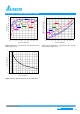
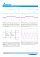
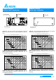
Figure 12: Input reflected ripple current, i
s
, through a 12µH
source inductor at nominal input voltage and max load current
(20 mA/div
,
2us/div).
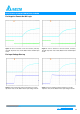
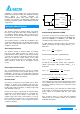
Figure 13: Output voltage noise and ripple measurement test
setup.
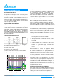
0
1
2
3
4
5
6
0 5 10 15 20 25 30 35
Output Current (A)
Output Voltage (V)
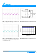
Figure 14: Output voltage ripple at nominal input voltage and
max load current (50 mV/div, 2us/div)
Load capacitance: 1µF ceramic capacitor and 10µF tantalum
capacitor. Bandwidth: 20 MHz.
Figure 15: Output voltage vs. load current showing typical
current limit curves and converter shutdown points.