
Datasheet

DS_E36SC05025_08162013 E-mail: DCDC@delta.com.tw
http://www.deltaww.com/dcdc
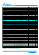
P5
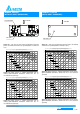
ELECTRICAL CHARACTERISTICS CURVES
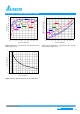
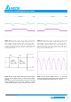
Figure 8: Output voltage response to step-change in load current
(50%-75%-50% of Io, max; di/dt = 0.1A/µs; Vin is 24V). Load cap:
10µF tantalum capacitor and 1µF ceramic capacitor. Top Trace:
Vout (0.2V/div, 100us/div), Bottom Trace:Iout (10A/div). Scope
measurement should be made using a BNC cable (length shorter than
20 inches). Position the load between 51 mm to 76 mm (2 inches to 3
inches) from the module
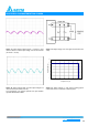
Figure 9: Output voltage response to step-change in load current
(50%-75%-50% of Io, max; di/dt = 0.1A/µs; Vin is 48V). Load cap:
10µF tantalum capacitor and 1µF ceramic capacitor. Top Trace:
Vout (0.2V/div, 100us/div), Bottom Trace: Iout (10A/div). Scope
measurement should be made using a BNC cable (length shorter
than 20 inches). Position the load between 51 mm to 76 mm (2
inches to 3 inches) from the module
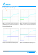
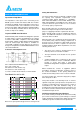
Figure 10: Test set-up diagram showing measurement points
for Input Terminal Ripple Current and Input Reflected Ripple
Current.
Note: Measured input reflected-ripple current with a simulated
source Inductance (L
TEST
) of 12 μH. Capacitor Cs offset
possible battery impedance. Measure current as shown above.
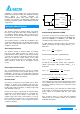
Figure 11: Input Terminal Ripple Current, i
c
, at max output
current and nominal input voltage with 12µH source impedance
and 33µF electrolytic capacitor (500 mA/div
,
2us/div).