
Integration Guide


Table Of Contents
- Preface
- Contents
- 1 System description
- 1.1 Overview
- 1.2 Architecture
- 1.3 Pin-out
- 1.4 Operating modes
- 1.5 Power management
- 1.6 System functions
- 1.7 RF connection
- 1.8 SIM interface
- 1.9 Serial Communication
- 1.10 Audio
- 1.11 ADC input (LEON-G100 only)
- 1.12 General Purpose Input/Output (GPIO)
- 1.13 M2M Setup Schematic Example
- 1.14 Approvals
- 2 Design-In
- 3 Handling and soldering
- 4 Product Testing
- Appendix
- A Extra Features
- B Glossary
- Related documents
- Revision history
- Contact
LEON-G100/G200 - System Integration Manual
GSM.G1-HW-09002-F3 Preliminary Design-In
Page 80 of 101
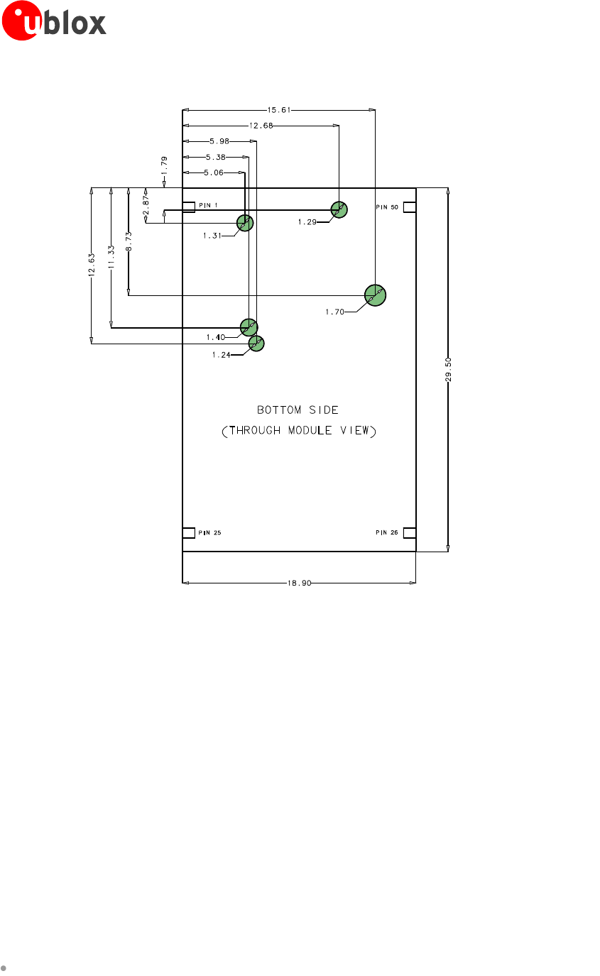
Figure 48: Signals keep-out below data module on application motherboard due to GND opening on data module bottom layer
for internal RF signals
Routing below LEON-G100/G200 on application motherboard is generally possible but not recommended: in
addition to the required keep-out defined before, consider that the insulation offered by the solder mask
painting may be weakened corresponding to micro-vias on LEON-G100/G200 bottom layer, thus increasing the
risk of short to GND if the application motherboard has unprotected signal routing on same coordinates.
2.2.3 Placement
Optimize placement for minimum length of RF line and closer path from DC source for VCC.
2.3 Module thermal resistance
The Case-to-Ambient thermal resistance (R
C-A
) of the module, with the LEON-G100/G200 mounted on a 130 x
110 x 1.6 mm FR4 PCB with a high coverage of copper (e.g. the EVK-G25H evaluation kit) in still air conditions is
equal to 14°C/W.
With this Case-to-Ambient thermal resistance, the increase of the module temperature is:
Around 12°C when the module transmits at the maximum power level during a GSM call in the GSM/EGSM
bands