
Integration Guide


Table Of Contents
- Preface
- Contents
- 1 System description
- 1.1 Overview
- 1.2 Architecture
- 1.3 Pin-out
- 1.4 Operating modes
- 1.5 Power management
- 1.6 System functions
- 1.7 RF connection
- 1.8 SIM interface
- 1.9 Serial Communication
- 1.10 Audio
- 1.11 ADC input (LEON-G100 only)
- 1.12 General Purpose Input/Output (GPIO)
- 1.13 M2M Setup Schematic Example
- 1.14 Approvals
- 2 Design-In
- 3 Handling and soldering
- 4 Product Testing
- Appendix
- A Extra Features
- B Glossary
- Related documents
- Revision history
- Contact
LEON-G100/G200 - System Integration Manual
GSM.G1-HW-09002-F3 Preliminary Design-In
Page 78 of 101
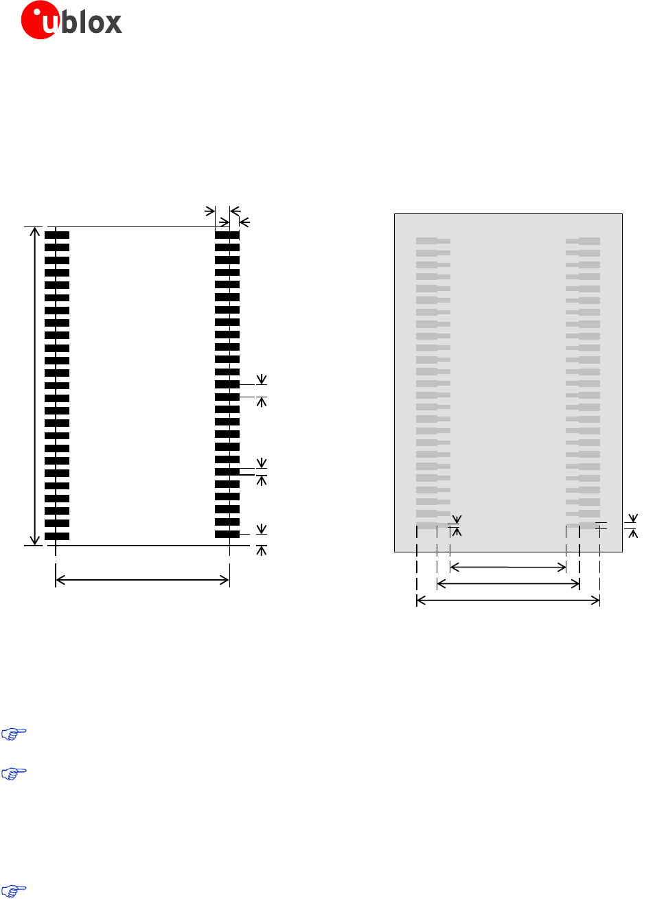
2.2.2 Footprint and paste mask
Figure 45 and Figure 46 describe the footprint and provide recommendations for the paste mask for LEON
modules. These are recommendations only and not specifications. Note that the copper and solder masks have
the same size and position.
29.5 mm [1161.4 mil]
18.9 mm [744.1 mil]
0.8 mm [31.5 mil]
1.1 mm [43.3 mil]
1.55 mm [61.0 mil]
1.0 mm [39.3 mil]
0.8 mm [31.5 mil]
Figure 45: LEON-G100/G200 footprint
21.3 mm [838.6 mil]
18.9 mm [744.1 mil]
Stencil: 120 µm
17.1 mm [673.2 mil]
0.6 mm
[23.6 mil]
0.8 mm [31.5 mil]
Figure 46: LEON-G100/G200 paste mask
To improve the wetting of the half vias, reduce the amount of solder paste under the module and increase the
volume outside of the module by defining the dimensions of the paste mask to form a T-shape (or equivalent)
extending beyond the Copper mask. The solder paste should have a total thickness of 120 µm.
The paste mask outline needs to be considered when defining the minimal distance to the next
component.
The exact geometry, distances, stencil thicknesses and solder paste volumes must be adapted to the
specific production processes (e.g. soldering etc.) of the customer.
The bottom layer of LEON-G100/G200 shows some unprotected copper areas for GND and VCC signals, plus
GND keep-out for internal RF signals routing.
Consider “No-routing” areas for the LEON-G100/G200 footprint as follows:
1. Ground copper and signals keep-out below LEON-G100/G200 on Application Motherboard due to VCC
area, RF ANT pin and exposed GND pad on module bottom layer (see Figure 47).
2. Signals Keep-Out below module on Application Motherboard due to GND opening on LEON-G100/G200
bottom layer for internal RF signals (see Figure 48).