
Integration Guide


Table Of Contents
- Preface
- Contents
- 1 System description
- 1.1 Overview
- 1.2 Architecture
- 1.3 Pin-out
- 1.4 Operating modes
- 1.5 Power management
- 1.6 System functions
- 1.7 RF connection
- 1.8 SIM interface
- 1.9 Serial Communication
- 1.10 Audio
- 1.11 ADC input (LEON-G100 only)
- 1.12 General Purpose Input/Output (GPIO)
- 1.13 M2M Setup Schematic Example
- 1.14 Approvals
- 2 Design-In
- 3 Handling and soldering
- 4 Product Testing
- Appendix
- A Extra Features
- B Glossary
- Related documents
- Revision history
- Contact
LEON-G100/G200 - System Integration Manual
GSM.G1-HW-09002-F3 Preliminary Design-In
Page 74 of 101
The transmission line must be routed in a section of the PCB where minimal interference from noise sources
can be expected
Route ANT line far from other sensitive circuits as it is a source of electromagnetic interference
Avoid coupling with VCC routing and analog audio lines
Ensure solid metal connection of the adjacent metal layer on the PCB stack-up to main ground layer
Add GND vias around transmission line
Ensure no other signals are routed parallel to transmission line, or that other signals cross on adjacent metal
layer
If the distance between the transmission line and the adjacent GND area (on the same layer) does not
exceed 5 times the track width of the micro strip, use the “Coplanar Waveguide” model for 50 Ω
characteristic impedance calculation
Don’t route microstrip line below discrete component or other mechanics placed on top layer
When terminating transmission line on antenna connector (or antenna pad) it is very important to strictly
follow the connector manufacturer’s recommended layout
GND layer under RF connectors and close to buried vias should be cut out in order to remove stray
capacitance and thus keep the RF line 50 Ω. In most cases the large active pad of the integrated antenna or
antenna connector needs to have a GND keep-out (i.e. clearance) at least on first inner layer to reduce
parasitic capacitance to ground. Note that the layout recommendation is not always available from
connector manufacturer: e.g. the classical SMA Pin-Through-Hole needs to have GND cleared on all the
layers around the central pin up to annular pads of the four GND posts. Check 50 Ω impedance of ANT line
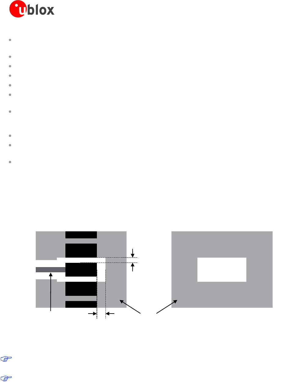
Min. 500 µm
Min.
250 um
Top layer Buried metal layer
GND
plane
Microstrip
50 Ω
Figure 44: GND keep-out area on the top layer around the ANT pad and on the buried metal layer below the ANT pad
Any RF transmission line on PCB should be designed for 50 Ω characteristic impedance.
Ensure no coupling occurs with other noisy or sensitive signals.
2.2.1.2 Main DC supply connection
The DC supply of LEON-G100/G200 modules is very important for the overall performance and functionality of
the integrated product. For detailed description check the design guidelines in section 1.5.2. Some main
characteristics are: