
Integration Guide


Table Of Contents
- Preface
- Contents
- 1 System description
- 1.1 Overview
- 1.2 Architecture
- 1.3 Pin-out
- 1.4 Operating modes
- 1.5 Power management
- 1.6 System functions
- 1.7 RF connection
- 1.8 SIM interface
- 1.9 Serial Communication
- 1.10 Audio
- 1.11 ADC input (LEON-G100 only)
- 1.12 General Purpose Input/Output (GPIO)
- 1.13 M2M Setup Schematic Example
- 1.14 Approvals
- 2 Design-In
- 3 Handling and soldering
- 4 Product Testing
- Appendix
- A Extra Features
- B Glossary
- Related documents
- Revision history
- Contact
LEON-G100/G200 - System Integration Manual
GSM.G1-HW-09002-F3 Preliminary Design-In
Page 72 of 101
Optimize placement for minimum length of RF line and closer path from DC source for VCC.
2.1.3 Antenna checklist
Antenna should have 50 Ω impedance, V.S.W.R less then 3:1, recommended 2:1 on operating bands in
deployment geographical area.
Antenna should have built in DC resistor to ground to get proper Antenna detection functionality.
2.2 Design Guidelines for Layout
The following design guidelines must be met for optimal integration of LEON-G100/G200 modules on the final
application board.
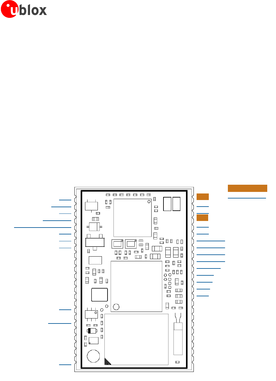
2.2.1 Layout guidelines per pin function
This section groups the LEON-G100/G200 pins by signal function and provides a ranking of importance in layout
design.
Pinout_Layout_R1.1(ppt)
GND
GND
ANT
GND
GND
MIC_BIAS1
MIC_GND1
MIC_GND2
MIC_BIAS2
Reserved
SPK_N
VCC
SPK_P
HS_P
GND
VSIM
SIM_RST
SIM_IO
SIM_CLK
SDA
SCL
I2S_RXD
I2S_CLK
I2S_TXD
I2S_WA
V_BCKP
GND
V_CHARGE
CHARGE_SENSE/ADC1
GND
GND
GND
DSR
RI
DCD
DTR
GND
RTS
CTS
TXD
RXD
GND
HS_DET
PWR_ON
GPIO1
GPIO2
RESET_N
Reserved
Reserved
GND
Very Important
Careful Layout
Common Practice
Legend:
Figure 43: Module pin-out with highlighted functions