
Integration Guide


Table Of Contents
- Preface
- Contents
- 1 System description
- 1.1 Overview
- 1.2 Architecture
- 1.3 Pin-out
- 1.4 Operating modes
- 1.5 Power management
- 1.6 System functions
- 1.7 RF connection
- 1.8 SIM interface
- 1.9 Serial Communication
- 1.10 Audio
- 1.11 ADC input (LEON-G100 only)
- 1.12 General Purpose Input/Output (GPIO)
- 1.13 M2M Setup Schematic Example
- 1.14 Approvals
- 2 Design-In
- 3 Handling and soldering
- 4 Product Testing
- Appendix
- A Extra Features
- B Glossary
- Related documents
- Revision history
- Contact
LEON-G100/G200 - System Integration Manual
GSM.G1-HW-09002-F3 Preliminary System description
Page 54 of 101
Reference
Description
Part Number - Manufacturer
R1, R2, R3
4.7 kΩ Resistor 0402 5% 0.1 W
RC0402JR-074K7L - Yageo Phycomp
U1
Voltage Regulator for GPS Receiver
See GPS Receiver Hardware Integration Manual
Table 19 - Component for DDC application circuit
1.9.2.3 DDC application circuit for LEON-G100/G200 upcoming version
This section applies to the upcoming FW/HW version of LEON-G100/G200.
The SDA and SCL lines can be used only to connect the LEON module to a u-blox GPS receiver: LEON DDC (I
2
C)
interface is enabled by the +UGPS AT command only (for more details refer to u-blox 2G GSM/GPRS AT
Commands Manual [2]).
GPIO2 is driven as an output by the +UGPS AT command to switch on or to switch off the u-blox GPS receiver,
connecting GPIO2 to the active-high enable pin (or the active-low shutdown pin) of the voltage regulator that
supplies the u-blox GPS module on the application board.
The pin #23 is driven as an input by the +UGPS AT command to sense when the u-blox GPS module is ready to
send data.
The pin #24 is driven as an output by the +UGPS AT command to provide a synchronization timing signal to the
u-blox GPS module.
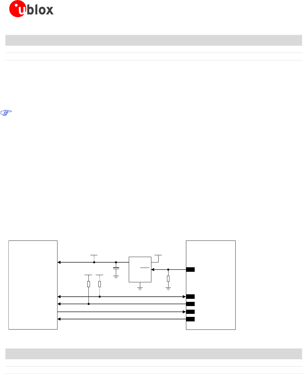
The application circuit for the connection of a LEON wireless module to a u-blox 3.0 V GPS receiver is illustrated
in Figure 35 and the suggested components are listed in Table 20. A pull-down resistor is mounted on the
GPIO2 line to avoid a switch on of the GPS module when the LEON module is switched-off and its digital pins
are tri-stated.
LEON-G100/G200
R1
INOUT
GND
GPS LDO
Regulator
SHDN
u-blox
3.0 V GPS receiver
SDA2
SCL2
R2
3V0 3V0
VMAIN3V0
U1
21
GPIO2
SDA
SCL
C1
TxD1
EXTINT0
31
30
23
24
VCC
R3
Figure 35: Application circuit for u-blox 3.0 V GPS receiver
Reference
Description
Part Number - Manufacturer
R1, R2, R3
4.7 kΩ Resistor 0402 5% 0.1 W
RC0402JR-074K7L - Yageo Phycomp
U1
Voltage Regulator for GPS Receiver
See GPS Receiver Hardware Integration Manual
Table 20: Components for application circuit for u-blox 3.0 V GPS receiver