
Integration Guide


Table Of Contents
- Preface
- Contents
- 1 System description
- 1.1 Overview
- 1.2 Architecture
- 1.3 Pin-out
- 1.4 Operating modes
- 1.5 Power management
- 1.6 System functions
- 1.7 RF connection
- 1.8 SIM interface
- 1.9 Serial Communication
- 1.10 Audio
- 1.11 ADC input (LEON-G100 only)
- 1.12 General Purpose Input/Output (GPIO)
- 1.13 M2M Setup Schematic Example
- 1.14 Approvals
- 2 Design-In
- 3 Handling and soldering
- 4 Product Testing
- Appendix
- A Extra Features
- B Glossary
- Related documents
- Revision history
- Contact
LEON-G100/G200 - System Integration Manual
GSM.G1-HW-09002-F3 Preliminary System description
Page 51 of 101
idle-mode to active-mode after 20 ms. The module will be forced in active-mode if the RTS input line is held in
the ON state.
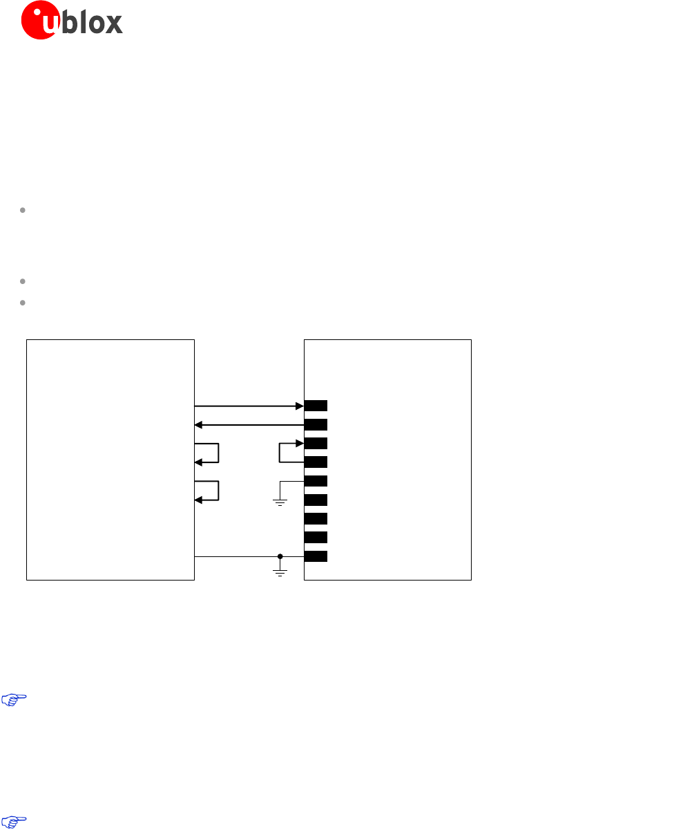
Providing the TxD and RxD lines only (not using the complete V24 link)
If the functionality of the CTS, RTS, DSR, DCD, RI and DTR lines is not required in the application, or the lines
are not available, the application circuit described in Figure 33 must be implemented:
Connect the module CTS output line to the module RTS input line, since the module requires RTS active
(low electrical level) if HW flow-control is enabled (AT&K3, that is the default setting), and CTS is active (low
electrical level) when the module is in active mode, the UART interface is enabled and the HW flow-control is
enabled
Connect the module DTR input line to GND, since the module requires DTR active (low electrical level)
Leave DSR, DCD and RI lines of the module unconnected and floating
LEON-G100/G200
(DCE)
TxD
Application Processor
(DTE)
RxD
RTS
CTS
DTR
DSR
RI
DCD
GND
15
TXD
12
DTR
16
RXD
13
RTS
14
CTS
9
DSR
10
RI
11
DCD
GND
Figure 33: UART interface application circuit with partial V.24 link (3-wire) in the DTE/DCE serial communication
If only TxD and RxD lines are provided as described in Figure 33 and HW flow-control is disabled (AT&K0), the
power saving will be enabled by AT+UPSV=1. The module enters active-mode 20 ms after a low-to-high
transition on the TxD input line; the recognition of the subsequent characters is guaranteed until the module is
in active-mode.
A data delivered by the DTE can be lost using this configuration and the following settings:
o HW flow-control enabled in the module (AT&K3, that is the default setting)
o Module power saving enabled by AT+UPSV=1
o HW flow-control disabled in the DTE
In this case the first character sent when the module is in idle-mode will be a wake-up character and
won’t be a valid communication character (refer to chapter 1.9.1.3 for the complete description).
If power saving is enabled the application circuit with the TxD and RxD lines only is not recommended.
During command mode the DTE must send to the module a wake-up character or a dummy “AT”
before each command line (refer to chapter 1.9.1.3 for the complete description), but during data mode
the wake-up character or the dummy “AT” would affect the data communication.