
Integration Guide


Table Of Contents
- Preface
- Contents
- 1 System description
- 1.1 Overview
- 1.2 Architecture
- 1.3 Pin-out
- 1.4 Operating modes
- 1.5 Power management
- 1.6 System functions
- 1.7 RF connection
- 1.8 SIM interface
- 1.9 Serial Communication
- 1.10 Audio
- 1.11 ADC input (LEON-G100 only)
- 1.12 General Purpose Input/Output (GPIO)
- 1.13 M2M Setup Schematic Example
- 1.14 Approvals
- 2 Design-In
- 3 Handling and soldering
- 4 Product Testing
- Appendix
- A Extra Features
- B Glossary
- Related documents
- Revision history
- Contact
LEON-G100/G200 - System Integration Manual
GSM.G1-HW-09002-F3 Preliminary System description
Page 50 of 101
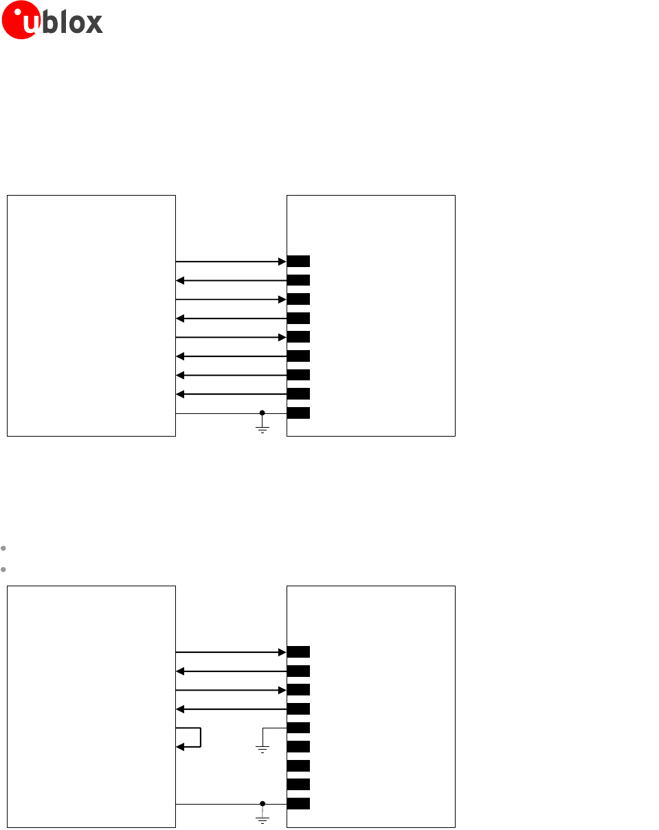
1.9.1.4 UART application circuits
Providing the full RS-232 functionality (using the complete V.24 link)
For complete RS-232 functionality conforming to ITU-T Recommendation [4] in DTE/DCE serial communication,
the complete UART interface of the module (DCE) must be connected to the DTE as described in Figure 31.
LEON-G100/G200
(DCE)
TxD
Application Processor
(DTE)
RxD
RTS
CTS
DTR
DSR
RI
DCD
GND
15
TXD
12
DTR
16
RXD
13
RTS
14
CTS
9
DSR
10
RI
11
DCD
GND
Figure 31: UART interface application circuit with complete V.24 link in the DTE/DCE serial communication
Providing the TxD, RxD, RTS and CTS lines only (not using the complete V.24 link)
If the functionality of the DSR, DCD, RI and DTR lines is not required in the application, or the lines are not
available, the application circuit described in Figure 32 must be implemented:
Connect the module DTR input line to GND, since the module requires DTR active (low electrical level)
Leave DSR, DCD and RI lines of the module unconnected and floating
LEON-G100/G200
(DCE)
TxD
Application Processor
(DTE)
RxD
RTS
CTS
DTR
DSR
RI
DCD
GND
15
TXD
12
DTR
16
RXD
13
RTS
14
CTS
9
DSR
10
RI
11
DCD
GND
Figure 32: UART interface application circuit with partial V.24 link (5-wire) in the DTE/DCE serial communication
If only TxD, RxD, RTS and CTS lines are provided as described in Figure 32 the procedure to enable the power
saving depends on the HW flow-control status. If HW flow-control is enabled (AT&K3, that is the default setting)
the power saving will be activated by AT+UPSV=1. Through this configuration, when the module is in idle-mode,
a data transmitted by the DTE will be buffered by the DTE and will be correctly received by the module when
active-mode is entered.
If the HW flow-control is disabled (AT&K0), the power saving can be enabled by AT+UPSV=2. The module is in
idle-mode until a high-to-low (i.e. OFF-to-ON) transition on the RTS input line will switch the module from