
Integration Guide


Table Of Contents
- Preface
- Contents
- 1 System description
- 1.1 Overview
- 1.2 Architecture
- 1.3 Pin-out
- 1.4 Operating modes
- 1.5 Power management
- 1.6 System functions
- 1.7 RF connection
- 1.8 SIM interface
- 1.9 Serial Communication
- 1.10 Audio
- 1.11 ADC input (LEON-G100 only)
- 1.12 General Purpose Input/Output (GPIO)
- 1.13 M2M Setup Schematic Example
- 1.14 Approvals
- 2 Design-In
- 3 Handling and soldering
- 4 Product Testing
- Appendix
- A Extra Features
- B Glossary
- Related documents
- Revision history
- Contact
LEON-G100/G200 - System Integration Manual
GSM.G1-HW-09002-F3 Preliminary System description
Page 48 of 101
AT+UPSV=2: power saving enabled and controlled by the RTS line
The module behavior is the same as for +UPSV=1 case if the RTS line is set to OFF by the DTE.
When an OFF-to-ON transition occurs on the RTS input line, the module switches from idle-mode to
active-mode after 20 ms and then the module doesn’t enter the idle-mode until the RTS input line is held in the
ON state. This configuration can only be enabled with the module HW flow control disabled.
Even if HW flow control is disabled, if the RTS line is set to OFF by the DTE, the CTS line is set by the
module accordingly to its power saving configuration (like for +UPSV=1 with HW flow control enabled).
When the RTS line is set to OFF by the DTE, the timeout to enter idle-mode from the last data received
at the serial port during the active-mode is the one previously set with the AT+UPSV=1 configuration or
it is the default value.
Wake up from idle-mode to active-mode via data reception
If a data is transmitted by the DTE during the module idle-mode, it will be lost (not correctly received by the
module) in the following cases:
+UPSV=1 with hardware flow control disabled
+UPSV=2 with hardware flow control disabled and RTS line set to OFF
When the module is in idle-mode, the TxD input line of the module is always configured to wake up the module
from idle-mode to active-mode via data reception: when a low-to-high transition occurs on the TxD input line, it
causes the wake-up of the system. The module switches from idle-mode to active-mode after 20 ms from the
first data reception: this is the “wake up time” of the module. As a consequence, the first character sent when
the module is in idle-mode (i.e. the wake up character) won’t be a valid communication character because it
can’t be recognized, and the recognition of the subsequent characters is guaranteed only after the complete
wake-up (i.e. after 20 ms).
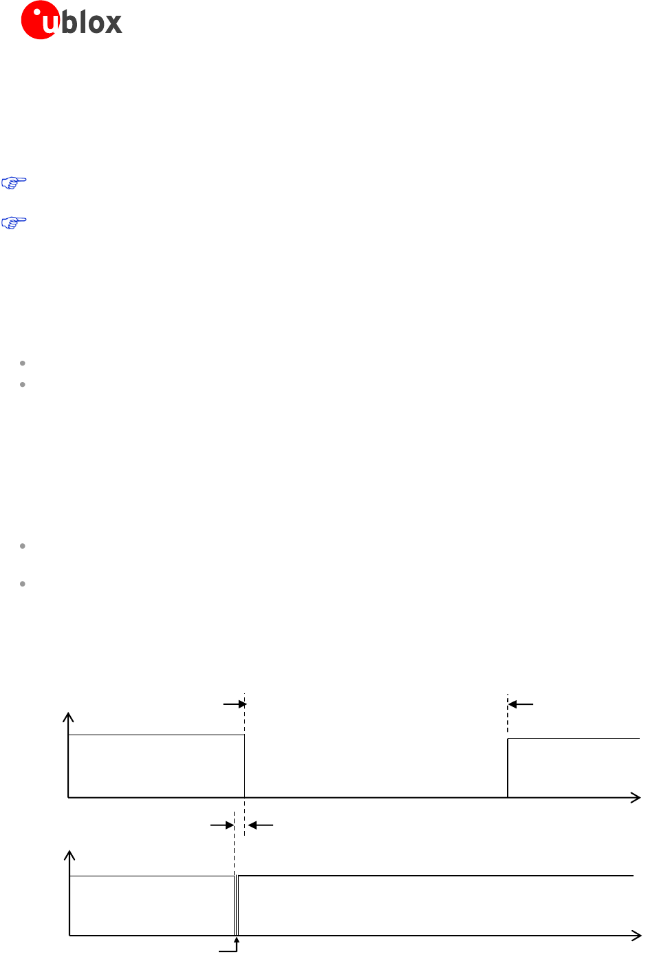
Figure 29 and Figure 30 show an example of common scenarios and timing constraints:
HW flow control set in the DCE, and no HW flow control set in the DTE, needed to see the CTS line
changing on DCE
Power saving configuration is active and the timeout from last data received to idle-mode start is set to 2000
frames (AT+UPSV=1,2000)
Figure 29 shows the case where DCE is in idle mode and a wake-up is forced. In this scenario the only character
sent by the DTE is the wake-up character; as a consequence, the DCE will return to idle-mode when the timeout
from last data received expires. (2000 frames without data reception).
CTS OFF
CTS ON
Active mode is held for 2000 GSM frames (~9.2 s)
time
Wake up time: up to 15.6 ms
time
TxD
module
input
Wake up character
Not recognized by DCE
Figure 29: Wake-up via data reception without further communication