
Integration Guide


Table Of Contents
- Preface
- Contents
- 1 System description
- 1.1 Overview
- 1.2 Architecture
- 1.3 Pin-out
- 1.4 Operating modes
- 1.5 Power management
- 1.6 System functions
- 1.7 RF connection
- 1.8 SIM interface
- 1.9 Serial Communication
- 1.10 Audio
- 1.11 ADC input (LEON-G100 only)
- 1.12 General Purpose Input/Output (GPIO)
- 1.13 M2M Setup Schematic Example
- 1.14 Approvals
- 2 Design-In
- 3 Handling and soldering
- 4 Product Testing
- Appendix
- A Extra Features
- B Glossary
- Related documents
- Revision history
- Contact
LEON-G100/G200 - System Integration Manual
GSM.G1-HW-09002-F3 Preliminary System description
Page 39 of 101
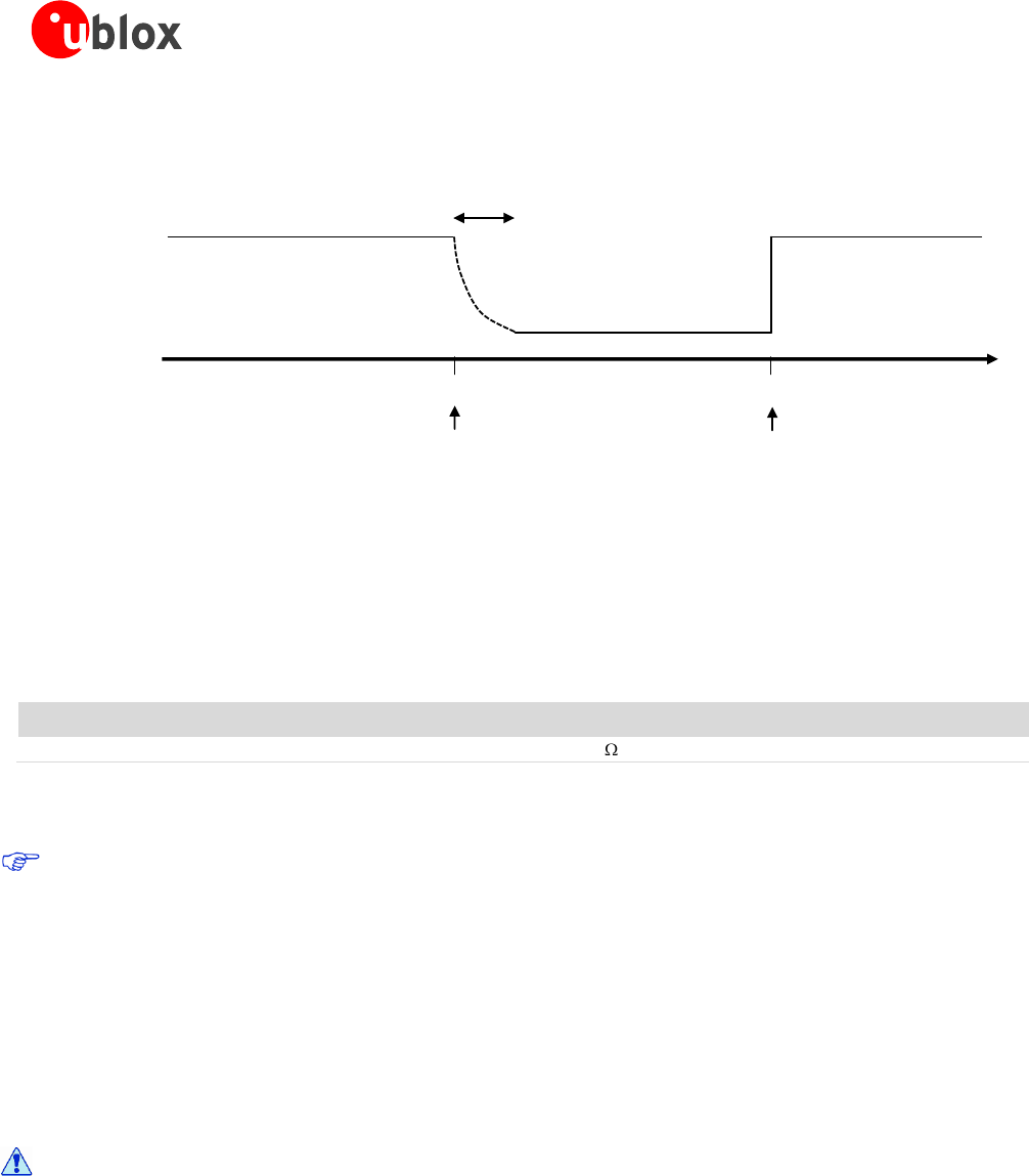
Depends on the
pull-down strength
(~35 µs with 680 k)
time [µs]
1600
LOW = 0 V
HIGH = 1.88 V
Reset state start Reset state end
RESET_N
Figure 23: RESET_N behavior due to an internal reset
1.7 RF connection
The ANT pin has 50 Ω nominal impedance and must be connected to the antenna through a 50 Ω transmission
line to allow transmission and reception of radio frequency (RF) signals in the GSM operating bands.
Name
Description
Remarks
ANT
RF antenna
50 nominal impedance.
Table 13: Antenna pin
ANT port ESD rating is 4 kV (contact discharge). A higher protection level could be required if the line is
externally accessible on the application board. A higher protection level can be achieved with an external
high pass filter, consists of a 15 pF capacitor (e.g. Murata GRM1555C1H150JA01) and a 39 nH coil (e.g.
Murata LQG15HN39NJ02) connected to the ANT port. Note that antenna detection functionality will be
not provided implementing this high pass filter for ESD protection on the ANT port.
Choose an antenna with optimal radiating characteristics for the best electrical performance and overall module
functionality. An internal antenna, integrated on the application board, or an external antenna, connected to the
application board through a proper 50 Ω connector, can be used. See section 2.4 and 2.2.1.1 for further details
regarding antenna guidelines.
The recommendations of the antenna producer for correct installation and deployment (PCB
layout and matching circuitry) must be followed.
If an external antenna is used, the PCB-to-RF-cable transition must be implemented using either a suitable 50 Ω
connector, or an RF-signal solder pad (including GND) that is optimized for 50 Ω characteristic impedance.
If antenna supervisor functionality is required, the antenna should have built in DC diagnostic resistor to ground
to get proper antenna detection functionality (See section 2.4.3 Antenna detection functionality).