
Integration Guide


Table Of Contents
- Preface
- Contents
- 1 System description
- 1.1 Overview
- 1.2 Architecture
- 1.3 Pin-out
- 1.4 Operating modes
- 1.5 Power management
- 1.6 System functions
- 1.7 RF connection
- 1.8 SIM interface
- 1.9 Serial Communication
- 1.10 Audio
- 1.11 ADC input (LEON-G100 only)
- 1.12 General Purpose Input/Output (GPIO)
- 1.13 M2M Setup Schematic Example
- 1.14 Approvals
- 2 Design-In
- 3 Handling and soldering
- 4 Product Testing
- Appendix
- A Extra Features
- B Glossary
- Related documents
- Revision history
- Contact
LEON-G100/G200 - System Integration Manual
GSM.G1-HW-09002-F3 Preliminary System description
Page 29 of 101
16
15.0
14
13
12
11
10
9
8
7
6
5
4
3
2
1
0
800700500
400
3002001000 900 1000 1100
mA
V
5.6
600
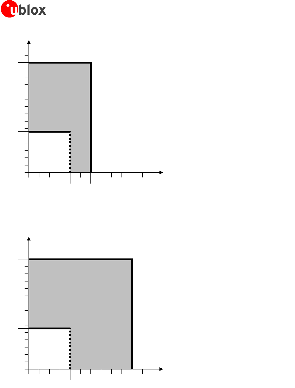
Figure 15: Valid area for the charger V-I output characteristics using a battery with a max DC charging current equal to 600 mA
For example, Figure 16 shows the valid area for the charger V-I output characteristics using a battery with a
maximum DC charging current greater than 1000 mA: the maximum acceptable charging current is defined by
the module requirement (1000 mA).
16
15.0
14
13
12
11
10
9
8
7
6
5
4
3
2
1
0
800700500
400
3002001000 900600 1100
mA
V
5.6
1000
Figure 16: Valid area for the charger V-I output characteristics using a battery with a max DC charging current greater than 1 A