
Integration Guide


Table Of Contents
- Preface
- Contents
- 1 System description
- 1.1 Overview
- 1.2 Architecture
- 1.3 Pin-out
- 1.4 Operating modes
- 1.5 Power management
- 1.6 System functions
- 1.7 RF connection
- 1.8 SIM interface
- 1.9 Serial Communication
- 1.10 Audio
- 1.11 ADC input (LEON-G100 only)
- 1.12 General Purpose Input/Output (GPIO)
- 1.13 M2M Setup Schematic Example
- 1.14 Approvals
- 2 Design-In
- 3 Handling and soldering
- 4 Product Testing
- Appendix
- A Extra Features
- B Glossary
- Related documents
- Revision history
- Contact
LEON-G100/G200 - System Integration Manual
GSM.G1-HW-09002-F3 Preliminary System description
Page 24 of 101
~30 ms
IDLE MODE ACTIVE MODE IDLE MODE
500-700 µA
8-10 mA
20-22 mA
~150 mA
Active Mode
Enabled
Idle Mode
Enabled
PLL
Enabled
RX+DSP
Enabled
500-700 µA
~150 mA
0.44-2.09 s
IDLE MODE
~30 ms
ACTIVE MODE
Time [s]
Current [mA]
150
100
50
0
Time [ms]
Current [mA]
150
100
50
0
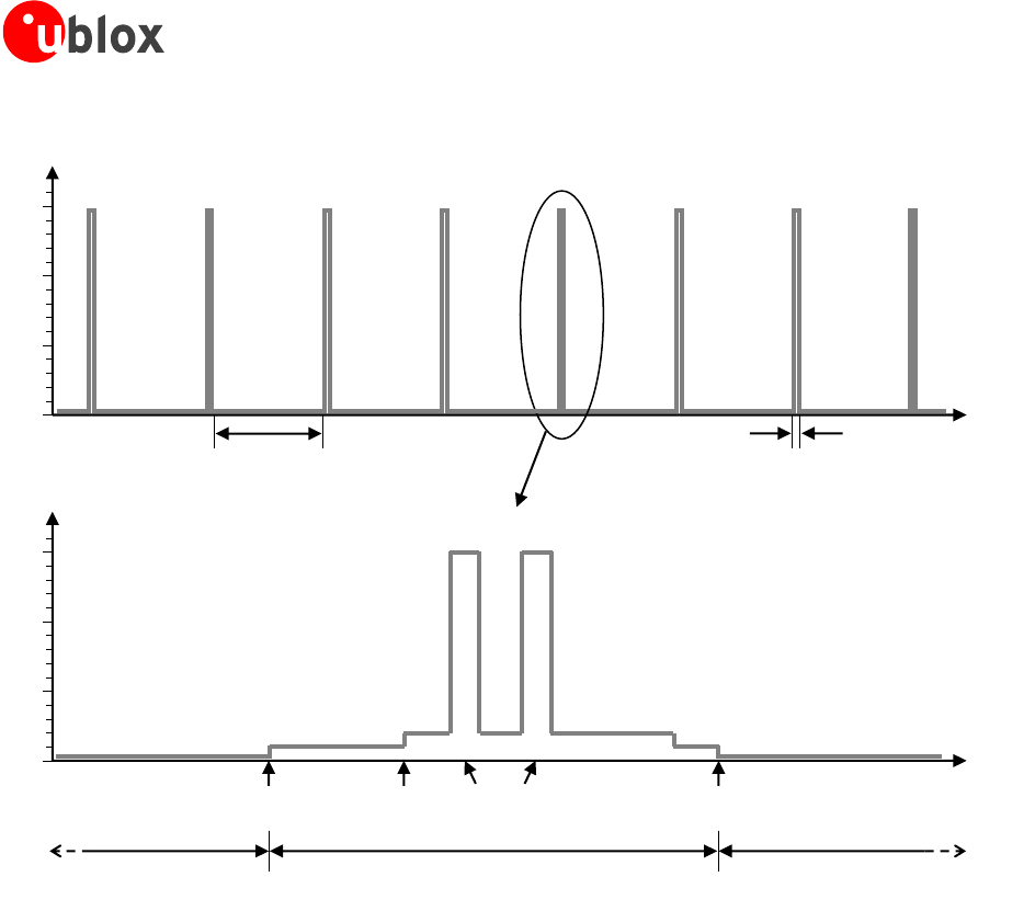
Figure 12: Description of the VCC current consumption profile versus time when power saving is enabled: the module is in idle
mode and periodically wakes up to active mode to monitor the paging channel for paging block reception
1.5.3.3 Current consumption profiles – Fixed active mode (power saving disabled)
Power saving configuration is by default disabled, or it can be disabled using the appropriate AT command (refer
to u-blox 2G GSM/GPRS AT Commands Manual [2], AT+UPSV command). When power saving is disabled, the
module doesn’t automatically enter idle-mode whenever possible: the module remains in active mode.
The module processor core is activated during active-mode, and the 26 MHz reference clock frequency is used.
An example of the current consumption profile of the data module when power saving is disabled is shown in
Figure 13: the module is registered with the network, active-mode is maintained, and the receiver and the DSP
are periodically activated to monitor the paging channel for paging block reception.