
Integration Guide


Table Of Contents
- Preface
- Contents
- 1 System description
- 1.1 Overview
- 1.2 Architecture
- 1.3 Pin-out
- 1.4 Operating modes
- 1.5 Power management
- 1.6 System functions
- 1.7 RF connection
- 1.8 SIM interface
- 1.9 Serial Communication
- 1.10 Audio
- 1.11 ADC input (LEON-G100 only)
- 1.12 General Purpose Input/Output (GPIO)
- 1.13 M2M Setup Schematic Example
- 1.14 Approvals
- 2 Design-In
- 3 Handling and soldering
- 4 Product Testing
- Appendix
- A Extra Features
- B Glossary
- Related documents
- Revision history
- Contact
LEON-G100/G200 - System Integration Manual
GSM.G1-HW-09002-F3 Preliminary System description
Page 21 of 101
Maximum pulse and DC discharge current: the no-rechargeable battery with its output circuit has to be
capable to deliver 2.5 A current pulses with 1/8 duty cycle to VCC pin and has to be capable to deliver a DC
current greater than the module maximum average current consumption to VCC pin. Note that the
maximum pulse and the maximum DC discharge current is not always reported in batteries data sheet, but
the maximum DC discharge current is typically almost equal to the battery capacity in Ampere-hours divided
by 1 hour
DC series resistance: the no-rechargeable battery with its output circuit has to be capable to avoid a VCC
voltage drop greater than 400 mV during transmit bursts
Additional hints for the VCC supply application circuits
To reduce voltage drops, use a low impedance power source. The resistance of the power supply lines
(connected to VCC and GND pins of the module) on the application board and battery pack should also be
considered and minimized: cabling and routing must be as short as possible in order to minimize power losses.
To avoid undershoot and overshoot on voltage drops at the start and at the end of a transmit burst during a
GSM call (when current consumption on the VCC supply can rise up to 2.5 A in the worst case), place a 330 µF
low ESR capacitor (e.g. KEMET T520D337M006ATE045) located near VCC pin of LEON-G100/G200.
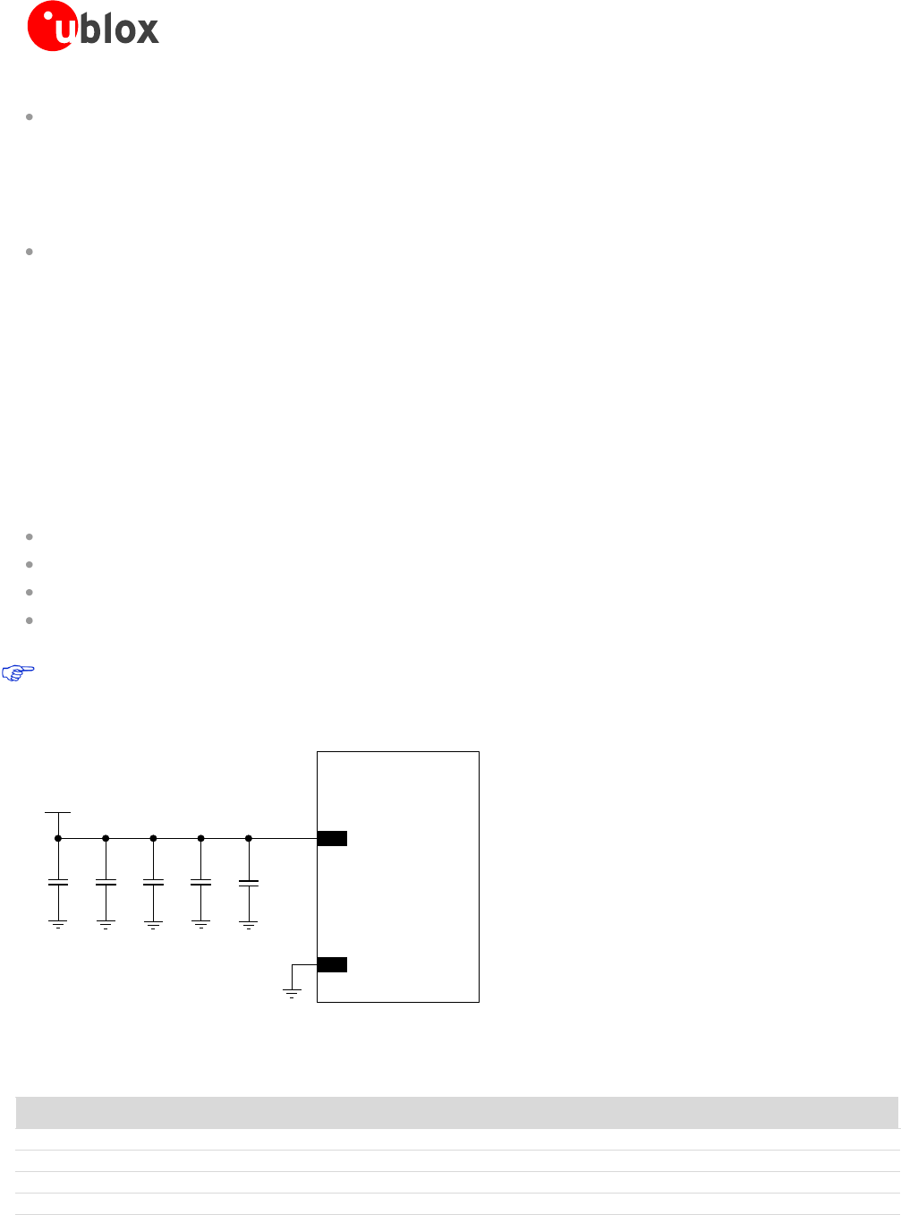
To reduce voltage ripple and noise, place near VCC pin of the LEON-G100/G200 the following components:
100 nF capacitor (e.g Murata GRM155R61A104K) to filter digital logic noises from clocks and data sources
10 nF capacitor (e.g. Murata GRM155R71C103K) to filter digital logic noises from clocks and data sources
10 pF capacitor (e.g. Murata GRM1555C1E100J) to filter transmission EMI in the DCS/PCS bands
39 pF capacitor (e.g. Murata GRM1555C1E390J) to filter transmission EMI in the GSM/EGSM bands
Note that the Figure 9 shows the complete configuration but the mounting of the each single
component depends on application design.
VBAT
C1 C4
LEON-G100
LEON-G200
50
VCC
GND
C3C2
C5
+
Figure 9: Suggested schematics design to reduce voltage ripple, noise and avoid undershoot and overshoot on voltage drops
Reference
Description
Part Number - Manufacturer
C1
330 µF Capacitor Tantalum D_SIZE 6.3 V 45 mΩ
T520D337M006ATE045 - KEMET
C2
100 nF Capacitor Ceramic X7R 0402 10% 16 V
GRM155R61A104KA01 - Murata
C3
10 nF Capacitor Ceramic X7R 0402 10% 16 V
GRM155R71C103KA01 - Murata
C4
39 pF Capacitor Ceramic C0G 0402 5% 25 V
GRM1555C1E390JA01 - Murata
C5
10 pF Capacitor Ceramic C0G 0402 5% 25 V
GRM1555C1E100JA01 - Murata
Table 7: Suggested components to reduce voltage ripple and noise and avoid undershoot and overshoot on voltage drops