
Integration Guide


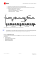


Table Of Contents
- Preface
- Contents
- 1 System description
- 1.1 Overview
- 1.2 Architecture
- 1.3 Pin-out
- 1.4 Operating modes
- 1.5 Power management
- 1.6 System functions
- 1.7 RF connection
- 1.8 SIM interface
- 1.9 Serial Communication
- 1.10 Audio
- 1.11 ADC input (LEON-G100 only)
- 1.12 General Purpose Input/Output (GPIO)
- 1.13 M2M Setup Schematic Example
- 1.14 Approvals
- 2 Design-In
- 3 Handling and soldering
- 4 Product Testing
- Appendix
- A Extra Features
- B Glossary
- Related documents
- Revision history
- Contact
LEON-G100/G200 - System Integration Manual
GSM.G1-HW-09002-F3 Preliminary System description
Page 16 of 101
o Voltage drop during transmit slots has to be lower than 400 mV
o Undershoot and overshoot at the start and at the end of transmit slots have to be not present
o Voltage ripple during transmit slots has to be:
lower than 100 mVpp if f
ripple
≤ 200 kHz
lower than 10 mVpp if 200 kHz < f
ripple
≤ 400 kHz
lower than 2 mVpp if f
ripple
> 400 kHz
Figure 4: Description of the VCC voltage profile versus time during a GSM call
Any degradation in power supply performance (due to losses, noise or transients) will directly affect the
RF performance of the module since the single external DC power source indirectly supplies all the
digital and analog interfaces, and also directly supplies the RF power amplifier (PA).
1.5.2.1 VCC application circuits
The LEON module must be supplied through the VCC pin by one (and only one) proper DC power supply from
the following:
Switching regulator
Low Drop-Out (LDO) linear regulator
Rechargeable Li-Ion battery
Primary (disposable) battery
Time
undershoot
overshoot
ripple
ripple
drop
Voltage
3.8 V
(typ)
RX
slot
unused
slot
unused
slot
TX
slot
unused
slot
unused
slot
MON
slot
unused
slot
RX
slot
unused
slot
unused
slot
TX
slot
unused
slot
unused
slot
MON
slot
unused
slot
GSM frame
4.615 ms
(1 frame = 8 slots)
GSM frame
4.615 ms
(1 frame = 8 slots)
RX
slot
unused
slot
unused
slot
TX
slot
unused
slot
unused
slot
MON
slot
unused
slot
RX
slot
unused
slot
unused
slot
TX
slot
unused
slot
unused
slot
MON
slot
unused
slot
GSM frame
4.615 ms
(1 frame = 8 slots)
GSM frame
4.615 ms
(1 frame = 8 slots)