
Integration Guide


Table Of Contents
- Preface
- Contents
- 1 System description
- 1.1 Overview
- 1.2 Architecture
- 1.3 Pin-out
- 1.4 Operating modes
- 1.5 Power management
- 1.6 System functions
- 1.7 RF connection
- 1.8 SIM interface
- 1.9 Serial Communication
- 1.10 Audio
- 1.11 ADC input (LEON-G100 only)
- 1.12 General Purpose Input/Output (GPIO)
- 1.13 M2M Setup Schematic Example
- 1.14 Approvals
- 2 Design-In
- 3 Handling and soldering
- 4 Product Testing
- Appendix
- A Extra Features
- B Glossary
- Related documents
- Revision history
- Contact
LEON-G100/G200 - System Integration Manual
GSM.G1-HW-09002-F3 Preliminary System description
Page 11 of 101
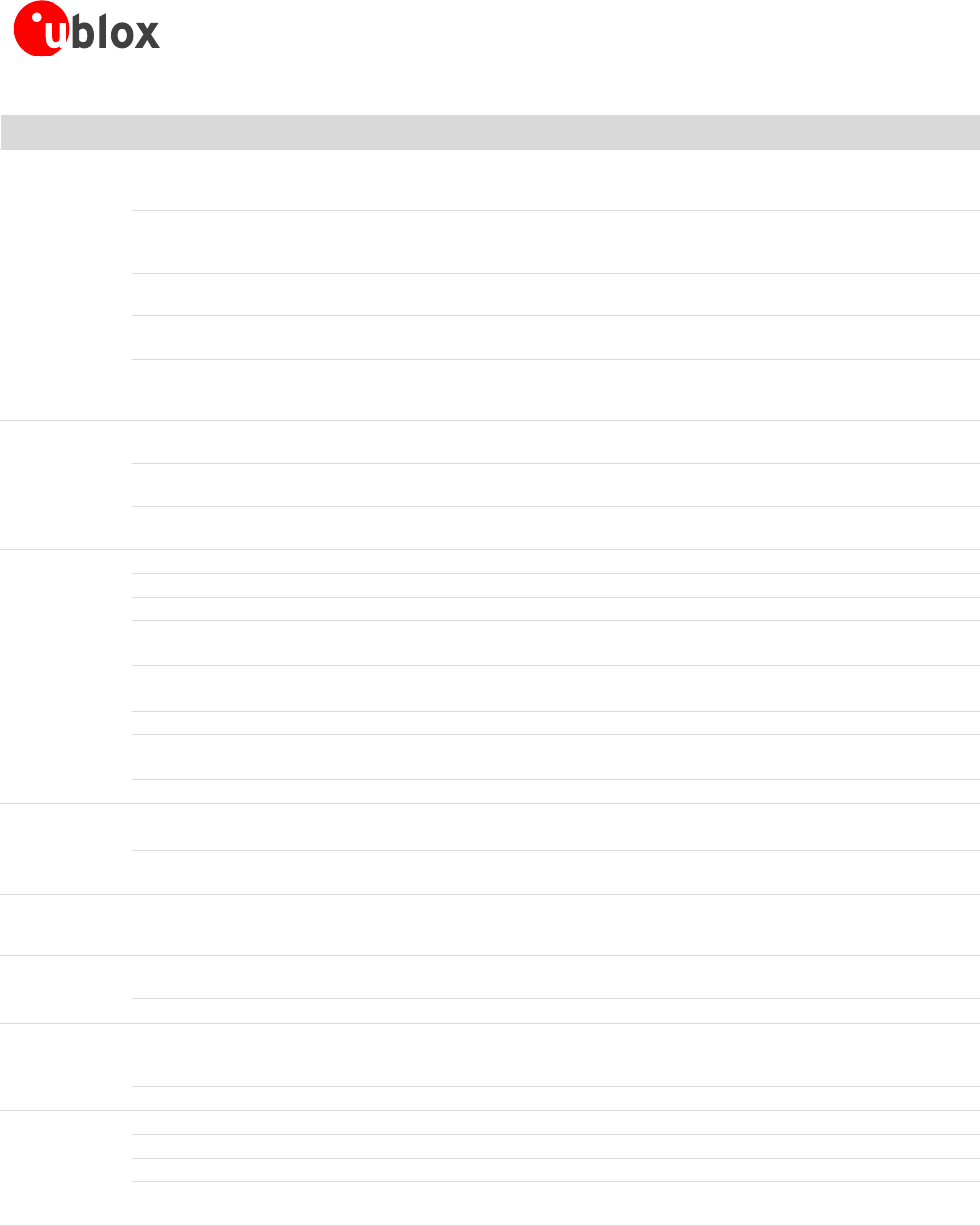
Function
Pin
No
I/O
Description
Remarks
SPK_N
39
O
Second speaker output
with power differential
analog audio output
This audio output is used when audio downlink
path is “Loudspeaker“. Audio pin: see section
1.10.1
MIC_BIAS2
41
I
Second microphone
analog signal input and
bias output
This audio input is used when audio uplink path is
set as “Headset Microphone“. Audio pin: see
section 1.10.1
MIC_GND2
42
I
Second microphone
analog reference
Local ground of second microphone. Audio pin:
see section 1.10.1
MIC_GND1
43
I
First microphone analog
reference
Local ground of the first microphone. Audio pin:
see section 1.10.1
MIC_BIAS1
44
I
First microphone analog
signal input and bias
output
This audio input is used when audio uplink path is
set as “Handset Microphone“. Audio pin: see
section 1.10.1
SIM
SIM_CLK
32
O
SIM clock
SIM interface: see section 1.8. Must meet SIM
specifications
SIM_IO
33
I/O
SIM data
SIM interface: see section 1.8. Internal 4.7k pull-up
to VSIM. Must meet SIM specifications
SIM_RST
34
O
SIM reset
SIM interface: see section 1.8. Must meet SIM
specifications
UART
DSR
9
O
UART data set ready
Circuit 107 (DSR) in V.24. See section 1.9.1.
RI
10
O
UART ring indicator
Circuit 125 (RI) in V.24. See section 1.9.1.
DCD
11
O
UART data carrier detect
Circuit 109 (DCD) in V.24. See section 1.9.1.
DTR
12
I
UART data terminal
ready
Internal active pull-up to 2.85 V enabled.
Circuit 108/2 (DTR) in V.24. See section 1.9.1.
RTS
13
I
UART ready to send
Internal active pull-up to 2.85 V enabled.
Circuit 105 (RTS) in V.24. See section 1.9.1.
CTS
14
O
UART clear to send
Circuit 106 (CTS) in V.24. See section 1.9.1.
TxD
15
I
UART transmitted data
Internal active pull-up to 2.85 V enabled.
Circuit 103 (TxD) in V.24. See section 1.9.1.
RxD
16
O
UART received data
Circuit 104 (RxD) in V.24. See section 1.9.1.
DDC
SCL
30
O
I
2
C bus clock line
Fixed open drain. External pull-up required.
See section 1.9.2
SDA
31
I/O
I
2
C bus data line
Fixed open drain. External pull-up required.
See section 1.9.2
ADC
ADC1
(LEON-G100)
5
I
ADC input
Resolution: 12 bits. See section 1.11; consider that
the impedance of this input changes depending on
the operative mode
GPIO
GPIO1
20
I/O
GPIO
See section 1.12. Add a test point to provide
access to the pin for debugging.
GPIO2
21
I/O
GPIO
See section 1.12
System
PWR_ON
19
I
Power-on input
PWR_ON pin has high input impedance.
Do not keep floating in noisy environment:
external pull-up required. See section 1.6.1
RESET_N
22
I/O
Reset signal
See section 1.6.3
Reserved
Reserved
23
Do not connect
Reserved
24
Do not connect
Reserved
40
Do not connect
Reserved
(LEON-G100)
4
Do not connect
Table 1: LEON-G100/G200 pin-out