
Integration Guide


Table Of Contents
- Preface
- Contents
- 1 System description
- 1.1 Overview
- 1.2 Architecture
- 1.3 Pin-out
- 1.4 Operating modes
- 1.5 Power management
- 1.6 System functions
- 1.7 RF connection
- 1.8 SIM interface
- 1.9 Serial Communication
- 1.10 Audio
- 1.11 ADC input (LEON-G100 only)
- 1.12 General Purpose Input/Output (GPIO)
- 1.13 M2M Setup Schematic Example
- 1.14 Approvals
- 2 Design-In
- 3 Handling and soldering
- 4 Product Testing
- Appendix
- A Extra Features
- B Glossary
- Related documents
- Revision history
- Contact
LEON-G100/G200 - System Integration Manual
GSM.G1-HW-09002-F3 Preliminary System description
Page 10 of 101
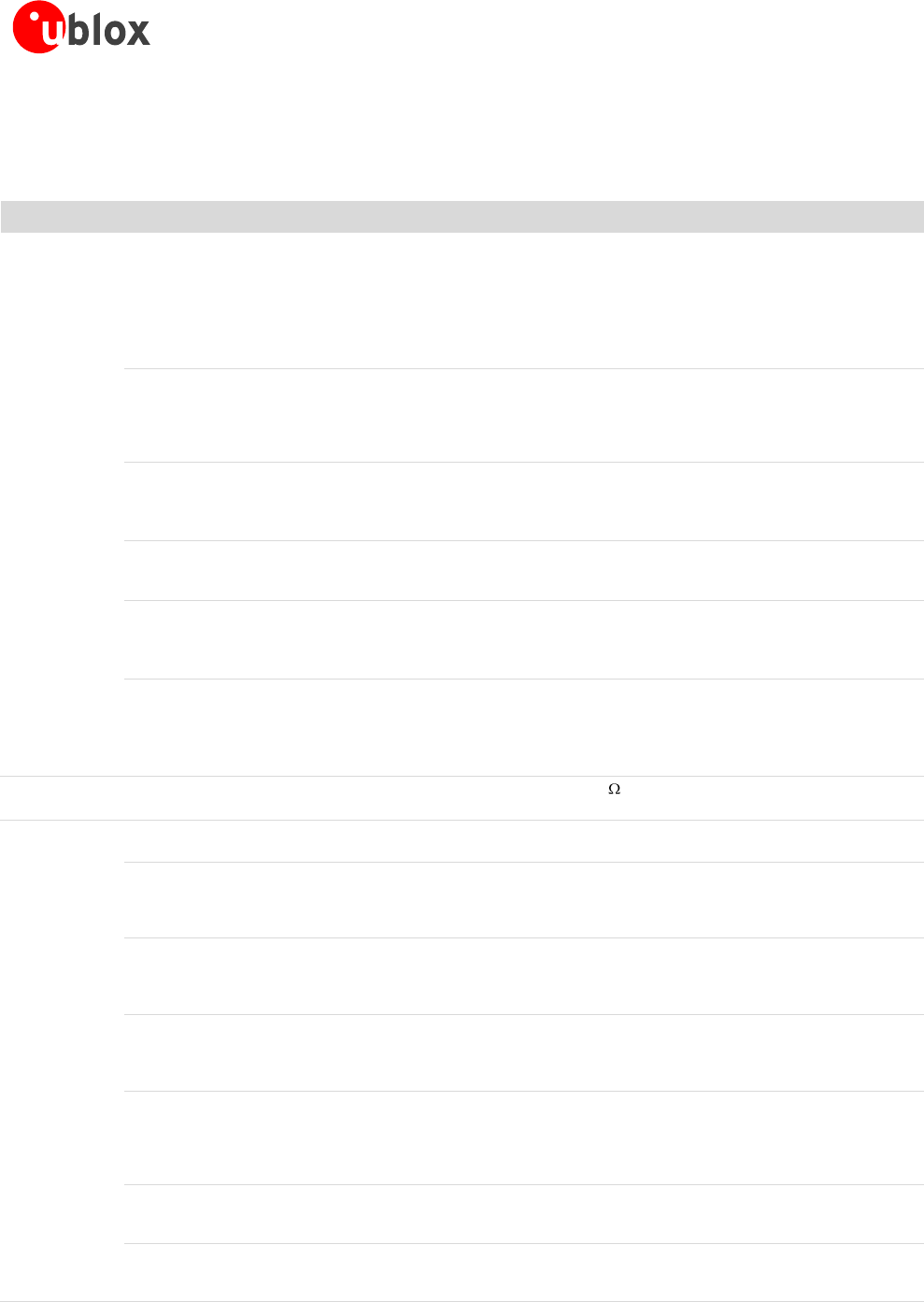
1.3 Pin-out
Table 1 describes the pin-out of LEON-G100/G200 modules, with pins grouped by function.
Function
Pin
No
I/O
Description
Remarks
Power
VCC
50
I
Module Supply
Clean and stable supply is required: low ripple and
low voltage drop must be guaranteed.
Voltage provided has to be always above the
minimum limit of the operating range.
Consider that there are large current spike in
connected mode, when a GSM call is enabled.
See section 1.5.2
GND
1, 3, 6,
7, 8, 17,
25, 36,
45, 46,
48, 49
N/A
Ground
GND pins are internally connected but good (low
impedance) external ground can improve RF
performances: all GND pins must be externally
connected to ground
V_BCKP
2
I/O
Real Time Clock supply
V_BCKP = 2.0 V (typical) generated by the module
to supply Real Time Clock when VCC supply
voltage is within valid operating range.
See section 1.5.5
VSIM
35
O
SIM supply
SIM supply automatically generated by the
module.
See section 1.8
V_CHARGE -
(LEON-G200)
4
I
Charger voltage supply
input
V_CHARGE and CHARGE_SENSE must be
externally connected.
The external supply used as charging source must
be voltage and current limited. See section 1.5.4
CHARGE_SENSE
(LEON-G200)
5
I
Charger voltage
measurement input
V_CHARGE and CHARGE_SENSE must be
externally connected.
The external supply used as charging source must
be voltage and current limited.
See section 1.5.4
RF
ANT
47
I/O
RF antenna
50 nominal impedance.
See section 1.7, 2.2.1.1 and 2.4
Audio
HS_DET
18
I
Headset detection input
Internal active pull-up to 2.85 V enabled.
See section 1.10.1.3
I2S_WA
26
O
I
2
S word alignment
I
2
S Interface: see section 1.10.2. Check device
specifications to ensure compatibility of supported
modes to LEON-G100/G200 module. Add a test
point to provide access to the pin for debugging.
I2S_TXD
27
O
I
2
S transmit data
I
2
S Interface: see section 1.10.2. Check device
specifications to ensure compatibility of supported
modes to LEON-G100/G200 module. Add a test
point to provide access to the pin for debugging.
I2S_CLK
28
O
I
2
S clock
I
2
S Interface: see section 1.10.2. Check device
specifications to ensure compatibility of supported
modes to LEON-G100/G200 module. Add a test
point to provide access to the pin for debugging.
I2S_RXD
29
I
I
2
S receive data
I
2
S Interface: see section 1.10.2. Internal active
pull-up to 2.85 V enabled. Check device
specifications to ensure compatibility of supported
modes to LEON-G100/G200 module. Add a test
point to provide access to the pin for debugging.
HS_P
37
O
First speaker output
with low power single-
ended analog audio
This audio output is used when audio downlink
path is “Normal earpiece“ or “Mono headset“
Audio pin: see section 1.10.1
SPK_P
38
O
Second speaker output
with high power
differential analog audio
This audio output is used when audio downlink
path is “Loudspeaker“. Audio pin: see section
1.10.1