
Datasheet


DTM63352B
2 GB - 240-Pin Registered ECC DDR2 DIMM with CMD/ADD Parity
Document 06555, Revision A, 16-Jul-2009, Dataram Corporation © 2009 Page 6
I
DD
Specifications and Conditions (Voltages referenced to V
ss
= 0 V)
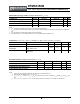
PARAMETER Symbol Test Condition
Max
Value
Unit
Operating One
Bank Active-
Precharge Current
I
DD
0
CKE is HIGH, /CS is HIGH between valid commands; Address
bus inputs are switching; Data bus inputs are switching.
1350
mA
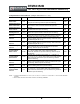
Operating One
Bank Active-Read-
Precharge Current
I
DD
1
I
OUT
= 0 mA; BL = 4, CL = 5 ns, AL = 0; CKE is HIGH, /CS is
HIGH between valid commands; Address bus inputs are
switching.
1530
mA
Precharge Power-
Down Current
I
DD
2P
All banks idle; CKE is LOW; Other control and address bus inputs
are stable; Data bus inputs are floating.
180
mA
Precharge Quiet
Standby Current
I
DD
2Q
All banks idle; CKE is HIGH, /CS is HIGH; Other control and
address bus inputs are stable; Data bus inputs are floating.
576
mA
Precharge Standby
Current
I
DD
2N
All banks idle; CKE is HIGH, /CS is HIGH; Other control and
address bus inputs are switching; Data bus inputs are switching.
810
mA
Active Power-Down
Current
I
DD
3P
All banks open; CKE is LOW; Other control and address bus
inputs are stable; Data bus inputs are floating. Fast Power-down
exit (Mode Register bit 12 = 0)
450
mA
Active Power-Down
Current
I
DD
3P
All banks open; CKE is LOW; Other control and address bus
inputs are stable; Data bus inputs are floating. Slow Power-down
exit (Mode Register bit 12 = 1)
216
mA
Active Standby
Current
I
DD
3N
All banks open; t
RAS
= 70 ms; CKE is HIGH, /CS is HIGH between
valid commands; Other control and address bus inputs are
switching; Data bus inputs are switching.
990
mA
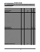
Operating Burst
Write Current
I
DD
4W
All banks open, Continuous burst writes; BL = 4, CL = 3; AL = 0;
t
RAS
= 70 ms, CKE is HIGH, /CS is HIGH between valid
commands; Address bus inputs are switching; Data bus inputs
are switching.
3240
mA
Operating Burst
Read Current
I
DD
4R
All banks open, Continuous burst reads, I
OUT
= 0 mA; BL = 4,
CL = 3, AL = 0; t
RAS
= 70 ms; CKE is HIGH, /CS is HIGH between
valid commands; Address bus inputs are switching; Data bus
inputs are switching.
3060
mA
Burst Refresh
Current
I
DD
5
Refresh command at every 7.8us; CKE is HIGH, /CS is HIGH
between valid commands; Other control and address bus inputs
are switching; Data bus inputs are switching.
3240
mA
Self Refresh
Current
I
DD
6
CK and /CK at 0 V; CKE ≤ 0.2 V; Other control and address bus
inputs are floating; Data bus inputs are floating.
180
mA
Operating Bank
Interleave Read
Current
I
DD
7
All bank interleaving reads, I
OUT
= 0 mA; BL = 4, CL = 3,
AL = 70ns; t
RRD
= 7.5 ns; CKE is HIGH, /CS is HIGH between
valid commands; Address bus inputs are stable during deselects;
Data bus inputs are switching.
4230
mA
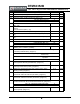
Notes: 1. For all I
DD
X measurements, t
CK
= 2.5 ns, t
RC
= 57 ns, t
RCD
= 12.5 ns, t
RAS
= 45 ns, and t
RP
= 12.5 ns unless otherwise
specified.
2. All I
DD
X values shown are worst-case maximums, considering all DRAMs.