
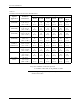
User manual


Preventive Maintenance
5-20 ProMaster 2500 User Manual
•
Pin Driver Board(s)
—Internally generated supply voltages serve as
inputs to the pin driver circuits from the waveform section of the
controller/waveform board. Control signals from the PCU
coprocessor on the controller/waveform board are also received and
used by the pin driver circuitry on the board to shape programming
waveforms. The pin driver controls the signal slew rates, current
source, and voltage levels required to provide precise programming
signals to the device installed in the programming module. These
signals are routed through the relay board to the SPA block and then
to the device.
•
Squirt Pin Assembly (SPA Block)
—This assembly has no active
circuitry but provides the shortest possible signal path between the
signal source and the device installed in the programming module.
•
Programming Modules
—Act as the interface between the device to
be tested/programmed and the PE. Modules are available for 300-
and 600-mil. (0.300-inch and 0.600-inch wide) DIP devices; 20-, 28-,
32-, 44-, 52-, 68-, and 84-pin PLCC devices; and 150-, 300-, 400-, and
500-mil SOIC devices. DIP modules use high quality contact sets to
establish contact with the device pins. PLCC devices are inserted into
a self-funneling programming block to achieve correct alignment.
The PE
Device List
disk (included in each update kit) lists the
supported devices and which programming module to use for a
specific device.
Self-calibration
The PE performs an automatic self-calibration of its supplies each time
the programmer is powered up and the self-test is run. The internal
power supply outputs +15V DC to the waveform section of the
controller/waveform board. This acts as the input to a precision voltage
regulator that outputs a +10V REF supply. This REF supply is used as the
input to digital-to-analog converter (DAC) controlled voltage and current
source circuits on the waveform board. One DAC outputs a comparator
reference (Comp Ref) voltage and the +10V REF supply is used to confirm
that the DAC output is correct.
The Comp Ref voltage is used, in turn, to verify the correct output voltage
levels of other supplies on the board. Additional comparator reference
levels are used on the pin driver board to confirm the output voltages as
they appear at the programming module. Overcurrent detection circuitry
is also tested during self-calibration. Waveform timing is derived from a
crystal-controlled programmable clock, which is driven off the main
system clock.
Programming Devices
The PE responds to computer remote control commands issued by
TaskLink, running on the PC. Data to be programmed into a device is
usually loaded from a master device or from a file. When a master device
is selected, the handler inserts the device into the programming module,
then the PE reads that data through the programming module contacts,
SPA pins, and pin drivers. Device data is stored in user RAM on the
controller/waveform board as an image of the fuses in the device. This
RAM data is preserved until a new device is loaded, RAM is changed by
the user, or the programmer is powered down.