
User`s guide


CY7C66013
C
CY7C66113
C
Document #: 38-08024 Rev. *B Page 60 of 61
© Cypress Semiconductor Corporation, 2006. The information contained herein is subject to change without notice. Cypress Semiconductor Corporation assumes no responsibility for the use
of any circuitry other than circuitry embodied in a Cypress product. Nor does it convey or imply any license under patent or other rights. Cypress products are not warranted nor intended to be
used for medical, life support, life saving, critical control or safety applications, unless pursuant to an express written agreement with Cypress. Furthermore, Cypress does not authorize its
products for use as critical components in life-support systems where a malfunction or failure may reasonably be expected to result in significant injury to the user. The inclusion of Cypress
products in life-support systems application implies that the manufacturer assumes all risk of such use and in doing so indemnifies Cypress against all charges.
Purchase of I
2
C components from Cypress, or one of its sublicensed Associated Companies, conveys a license under the Philips
I
2
C Patent Rights to use these components in an I
2
C system, provided that the system conforms to the I
2
C Standard Specification
as defined by Philips.
All product and company names mentioned in this document are the trademarks of their respective holders.
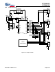
Figure 28-2. Plot of the Solder Mask (White Area)
0.017” dia
Solder Mask
Cu Fill
Cu Fill
PCB Material
PCB Material
0.013” dia
Via hole for thermally connecting the
QFN to the circuit board ground plane.
This figure only shows the top three layers of the
circuit board: Top Solder, PCB Dielectric, and
the Ground Plane
Figure 28-1. Cross-section of the Area Underneath the QFN Package