
User`s guide


CY7C66013
C
CY7C66113
C
Document #: 38-08024 Rev. *B Page 59 of 61
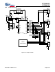
28.0 Quad Flat Package No Leads (QFN) Package Design Notes
Electrical contact of the part to the Printed Circuit Board (PCB) is made by soldering the leads on the bottom surface of the
package to the PCB. Hence, special attention is required to the heat transfer area below the package to provide a good thermal
bond to the circuit board. A Copper (Cu) fill is to be designed into the PCB as a thermal pad under the package. Heat is transferred
from the FX1 through the device’s metal paddle on the bottom side of the package. Heat from here, is conducted to the PCB at
the thermal pad. It is then conducted from the thermal pad to the PCB inner ground plane by a 5 x 5 array of via. A via is a plated
through hole in the PCB with a finished diameter of 13 mil. The QFN’s metal die paddle must be soldered to the PCB’s thermal
pad. Solder mask is placed on the board top side over each via to resist solder flow into the via. The mask on the top side also
minimizes outgassing during the solder reflow process.
For further information on this package design please refer to the application note Surface Mount Assembly of AMKOR’s
MicroLeadFrame (MLF) Technology. This application note can be downloaded from AMKOR’s website from the following URL
http://www.amkor.com/products/notes_papers/MLF_AppNote_0902.pdf. The application note provides detailed information on
board mounting guidelines, soldering flow, rework process, etc.
Figure 28-1 below displays a cross-sectional area underneath the package. The cross section is of only one via. The thickness
of the solder paste template should be 5 mil. It is recommended that “No Clean” type 3 solder paste is used for mounting the part.
Nitrogen purge is recommended during reflow.
Figure 28-2 is a plot of the solder mask pattern. This pad is thermally connected and is not electrically connected inside the chip.
To minimize EMI, this pad should be connected to the ground plane of the circuit board.
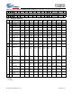
27.0 Package Diagrams (continued)
0.80[0.031]
7.70[0.303]
7.90[0.311]
A
C
1.00[0.039] MAX.
N
SEATING
PLANE
N
2
0.18[0.007]
0.50[0.020]
1
1
0.08[0.003]
0.50[0.020]
0.05[0.002] MAX.
2
(4X)
C
0.24[0.009]
0.20[0.008] REF.
0.80[0.031] MAX.
PIN1 ID
0°-12°
6.45[0.254]
8.10[0.319]
7.80[0.307]
6.55[0.258]
0.45[0.018]
0.20[0.008] R.
8.10[0.319]
7.90[0.311]
7.80[0.307]
7.70[0.303]
DIA.
0.28[0.011]
0.30[0.012]
6.55[0.258]
6.45[0.254]
0.60[0.024]
TOP VIEW
BOTTOM VIEW
SIDE VIEW
E-PAD
(PAD SIZE VARY
BY DEVICE TYPE)
51-85144-*D
56-Lead QFN 8 x 8 MM LF56A
Board Pad 4.7mm x 5.2 mm minimum
6.63mm x 6.63mm maximum