
User`s guide


CY7C66013
C
CY7C66113
C
Document #: 38-08024 Rev. *B Page 56 of 61
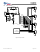
CLOCK
t
CYC
t
CL
t
CH
Figure 25-1. Clock Timing
90%
10%
90%
10%
D−
D+
t
r
t
r
Figure 25-2. USB Data Signal Timing
OE (P2.5, input)
DATA (output)
STB
(P2.4, input)
DReadyPin (P2.3, output)
Internal Write
Internal Addr
Port0
D[23:0]
t
OED
t
OEZ
t
RD
t
OEDR
CS (P2.6, input)
Int
(Shown for DRDY Polarity=0)
Interrupt Generated
(Ready)
Figure 25-3. HAPI Read by External Interface from USB Microcontroller