
User`s guide


CY7C66013
C
CY7C66113
C
Document #: 38-08024 Rev. *B Page 51 of 61
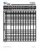
1 1 0 0 In x UC x UC UC UC UC 1 UC UC No ChangeNAK yes
Isochronous endpoint (In)
0 1 1 1 Out x UC x UC UC UC UC UC UC UC No Changeignore no
0 1 1 1 In x UC x UC UC UC UC 1 UC UC No ChangeTX yes
21.0 Register Summary
Addr
ess Register Name Bit 7 Bit 6 Bit 5 Bit 4 Bit 3 Bit 2 Bit 1 Bit 0
Read/Write
/Both
[5, 6, 7]
Default/
Reset
[8]
GPIO CONFIGURATION PORTS 0, 1, 2 AND 3
0x00 Port 0 Data P0.7 P0.6 P0.5 P0.4 P0.3 P0.2 P0.1 P0.0 bbbbbbbb 11111111
0x01 Port 1 Data P1.7 P1.6 P1.5 P1.4 P1.3 P1.2 P1.1 P1.0 bbbbbbbb 11111111
0x02 Port 2 Data P2.7 P2.6 P2.5 P2.4 P2.3 P2.2 P2.1 P2.0 bbbbbbbb 11111111
0x03 Port 3 Data Reserved P3.6
CY7C66113C
only
P3.5
CY7C66113C
only
P3.4 P3.3 P3.2 P3.1 P3.0 bbbbbbbb -1111111
0x04 Port 0 Interrupt
Enable
P0.7 Intr
Enable
P0.6 Intr
Enable
P0.5 Intr
Enable
P0.4 Intr
Enable
P0.3 Intr
Enable
P0.2 Intr
Enable
P0.1 Intr
Enable
P0.0 Intr
Enable
wwwwwwww 00000000
0x05 Port 1 Interrupt
Enable
P1.7 Intr
Enable
P1.6 Intr
Enable
P1.5 Intr
Enable
P1.4 Intr
Enable
P1.3 Intr
Enable
P1.2 Intr
Enable
P1.1 Intr
Enable
P1.0 Intr
Enable
wwwwwwww 00000000
0x06 Port 2 Interrupt
Enable
P2.7 Intr
Enable
P2.6 Intr
Enable
P2.5 Intr
Enable
P2.4 Intr
Enable
P2.3 Intr
Enable
P2.2 Intr
Enable
P2.1 Intr
Enable
P2.0 Intr
Enable
wwwwwwww 00000000
0x07 Port 3 Interrupt
Enable
Reserved
P3.6 Intr
Enable
CY7C66113C
only
P3.5 Intr
Enable
CY7C66113C
only
P3.4 Intr
Enable
P3.3 Intr
Enable
P3.2 Intr
Enable
P3.1 Intr
Enable
P3.0 Intr
Enable
wwwwwwww 00000000
0x08 GPIO
Configuration
Port 3
Config Bit
1
Port 3
Config Bit
0
Port 2
Config Bit
1
Port 2
Config Bit
0
Port 1
Config Bit
1
Port 1
Config Bit
0
Port 0
Config Bit
1
Port 0
Config Bit
0
bbbbbbbb 00000000
HAPI
I
2
C
0x09 HAPI/I
2
C
Configuration
I
2
C
Position
Reserved LEMPTY
Polarity
DRDY
Polarity
Latch
Empty
Data
Ready
Port Width
bit 1
Port Width
bit 0
b-bbrrbb 00000000
Endpoint A0, AI
and A2 Configuration
0x10 USB Device
Address A
Device
Address A
Enable
Device
Address
A Bit 6
Device
Address
A Bit 5
Device
Address
A Bit 4
Device
Address
A Bit 3
Device
Address
A Bit 2
Device
Address
A Bit 1
Device
Address
A Bit 0
bbbbbbbb 00000000
Endpoint A0, AI AND A2 Configuration
0x11 EP A0 Counter
Register
Data 0/1
To gg l e
Data
Valid
Byte
Count
Bit 5
Byte
Count
Bit 4
Byte
Count
Bit 3
Byte
Count
Bit 2
Byte
Count
Bit 1
Byte
Count
Bit 0
bbbbbbbb 00000000
0x12 EP A0 Mode
Register
Endpoint0
SETUP
Received
Endpoint0
IN
Received
Endpoint0
OUT
Received
ACK Mode Bit 3Mode Bit 2Mode Bit 1 Mode Bit 0bbbbbbbb 00000000
0x13 EP A1 Counter
Register
Data 0/1
To gg l e
Data Valid Byte
Count
Bit 5
Byte
Count
Bit 4
Byte
Count
Bit 3
Byte
Count
Bit 2
Byte
Count
Bit 1
Byte
Count
Bit 0
bbbbbbbb 00000000
0x14 EP A1 Mode
Register
STALL - - ACK Mode Bit 3Mode Bit 2 Mode Bit 1 Mode Bit 0 bbbbbbbb 00000000
0x15 EP A2 Counter
Register
Data 0/1
To gg l e
Data Valid Byte
Count
Bit 5
Byte
Count
Bit 4
Byte
Count
Bit 3
Byte
Count
Bit 2
Byte
Count
Bit 1
Byte
Count
Bit 0
bbbbbbbb 00000000
0x16 EP A2 Mode
Register
STALL - - ACK Mode Bit 3Mode Bit 2Mode Bit 1Mode Bit 0bbbbbbbb 00000000
USB-
CS
0x1F USB Status and
Control
Endpoint
Size
Endpoint
Mode
D+
Upstream
D–
Upstream
Bus
Activity
Control
Bit 2
Control
Bit 1
Control
Bit 0
bbrrbbbb -0xx0000
Notes:
5. B: Read and Write.
6. W: Write.
7. R: Read.
8. X: Unknown
Table 20-3. Details of Modes for Differing Traffic Conditions (see Table 20-2 for the decode legend) (continued)