
User`s guide


CY7C66013
C
CY7C66113
C
Document #: 38-08024 Rev. *B Page 32 of 61
Global Interrupt Enable Register ADDRESS 0X20
Bit 0: USB Bus RST Interrupt Enable
1 = Enable Interrupt on a USB Bus Reset; 0 = Disable interrupt on a USB Bus Reset (refer to section 16.3).
Bit 1: 128-µs Interrupt Enable
1 = Enable Timer interrupt every 128 µs; 0 = Disable Timer Interrupt for every 128 µs.
Bit 2: 1.024-ms Interrupt Enable
1= Enable Timer interrupt every 1.024 ms; 0 = Disable Timer Interrupt every 1.024 ms.
Bit 3: USB Hub Interrupt Enable
1 = Enable Interrupt on a Hub status change; 0 = Disable interrupt due to hub status change. (Refer to section 16.6.)
Bit 4: DAC Interrupt Enable
1 = Enable DAC Interrupt; 0 = Disable DAC interrupt.
Bit 5: GPIO Interrupt Enable
1 = Enable Interrupt on falling/rising edge on any GPIO; 0 = Disable Interrupt on falling/rising edge on any GPIO. (Refer to
sections 16.8, 9.1, and 9.2.)
Bit 6: I
2
C Interrupt Enable
1 = Enable Interrupt on I2C related activity; 0 = Disable I2C related activity interrupt. (Refer to section 16.9.)
Bit 7: Reserved.
USB Endpoint Interrupt Enable ADDRESS 0X21
Bit 0: EPA0 Interrupt Enable
1 = Enable Interrupt on data activity through endpoint A0; 0 = Disable Interrupt on data activity through endpoint A0.
Bit 1: EPA1 Interrupt Enable
1 = Enable Interrupt on data activity through endpoint A1; 0 = Disable Interrupt on data activity through endpoint A1.
Bit 2: EPA2 Interrupt Enable
1 = Enable Interrupt on data activity through endpoint A2; 0 = Disable Interrupt on data activity through endpoint A2.
Bit 3: EPB0 Interrupt Enable
1 = Enable Interrupt on data activity through endpoint B0; 0 = Disable Interrupt on data activity through endpoint B0.
Bit 4: EPB1 Interrupt Enable
1 = Enable Interrupt on data activity through endpoint B1; 0 = Disable Interrupt on data activity through endpoint B1.
Bit [7..5]: Reserved
During a reset, the contents the Global Interrupt Enable Register and USB End Point Interrupt Enable Register are cleared,
effectively, disabling all interrupts.
The interrupt controller contains a separate flip-flop for each interrupt. See Figure 16-3 for the logic block diagram of the interrupt
controller. When an interrupt is generated, it is first registered as a pending interrupt. It stays pending until it is serviced or a reset
occurs. A pending interrupt only generates an interrupt request if it is enabled by the corresponding bit in the interrupt enable
registers. The highest priority interrupt request is serviced following the completion of the currently executing instruction.
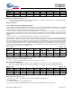
Bit #76543210
Bit Name Reserved I
2
C Interrupt
Enable
GPIO Interrupt
Enable
DAC Interrupt
Enable
USB Hub
Interrupt
Enable
1.024-ms
Interrupt
Enable
128-µs
Interrupt
Enable
USB Bus RST
Interrupt
Enable
Read/Write - R/W R/W R/W R/W R/W R/W R/W
Reset - 0000000
Figure 16-1. Global Interrupt Enable Register
Bit #76543210
Bit Name Reserved Reserved Reserved EPB1 Interrupt
Enable
EPB0 Interrupt
Enable
EPA2 Interrupt
Enable
EPA1 Interrupt
Enable
EPA0 Interrupt
Enable
Read/Write---R/WR/WR/WR/WR/W
Reset ---00000
Figure 16-2. USB Endpoint Interrupt Enable Register