
User`s manual
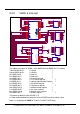

5.3 Serial Bus
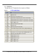
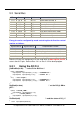
Pin Name
Default D/I/O mode Normal mode
J1.11 TO_0 D/I I/O_10 Timer output channel_0
J1.12 TO_1 D/I I/O_1 Timer output channel_1
J1.13 TI_0 D/I I/O_11 Timer input channel_0
J1.14 TI_1 D/I I/O_0 Timer input channel_1
J1.15 SCLK D/O I/O_26 UZI, don’t change to this mode
J1.16 DIO9 D/I I/O_9 A19, don’t change to this mode
J1.17 DIO4 D/I I/O_4 DT/R, don’t change to this mode
J1.18 DIO14 D/I I/O_14 MCS0, don’t change to this mode
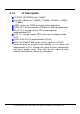
Every pin can be configured by mode control register & direction control
register as follows:
Mode control
register=0xff70
Direction control
register=0xff72
Programmable Function
0
0
Normal mode
0 1
D/I with pull-up/pull-down resistor (10K)
1 0
D/O
1 1
D/I without pull-up/pull-down register (10K)
After the I/O pins are configured, user can read /write to data register, 0xff74, to
access these I/O pins. Refer to Sec. 2.3.1 or Sec. 2.3.2 for demo program.
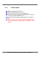
5.3.1 Using the D/I/O 4
SetDio4Dir(int dir) /* select D/I or D/O first */
{
if(dir){ /* set to input */
outport(0xff70,
ٛ
mport(0xff70)&(~(1<<4))); /* set MODE to 0 */
outport(0xff72,
ٛ
mport(0xff72)|(1<<4)); /* set DIR to 1 */
}
else { /* set to output */
outport(0xff70,
ٛ
mport(0xff70)|(1<<4)); /* set MODE to 1 */
outport(0xff72,
ٛ
mport(0xff72)&(~(1<<4))); /* set DIR to 0 */
}
}
OutDio4(int data) /* set the D/O_4 ON or
OFF */
{
if(data) /* set D/O_4 ON */
outport(0Xff74,
ٛ
mport(0Xff74)|(1<<4));
else /* set D/O_4 OFF */
outport(0Xff74,
ٛ
mport(0Xff74)&~(1<<4));
}
GetDio4(void) /* read the status of D/I_4 */
{
return
ٛ
mport(0Xff74)&0x0010;}
I/O Expansion Bus for 7188X/7188E User’s Manual, Jun/2004 v1.4, 7PH-000-14---30